How to Make PCB Circuit Board at Home
Do you want to make a Printed Circuit Board by yourself?
Maybe you are a student, due to the rules of the competition, you have to make PCB by yourself; maybe you are a PCB enthusiast and want to experience the fun of making PCB by yourself; maybe you are a beginner in PCB and want to DIY PCB to get more familiar with electronic circuits In short, you will make the PCB yourself for some reason. How to make PCB by yourself at home? If you want to DIY a PCB, it can be roughly divided into four steps: design, material preparation, production, and testing.
Step 1: design:
Before designing, you must first select the design software, you can choose the design software according to your own habits. Altium Designer is recommended here.
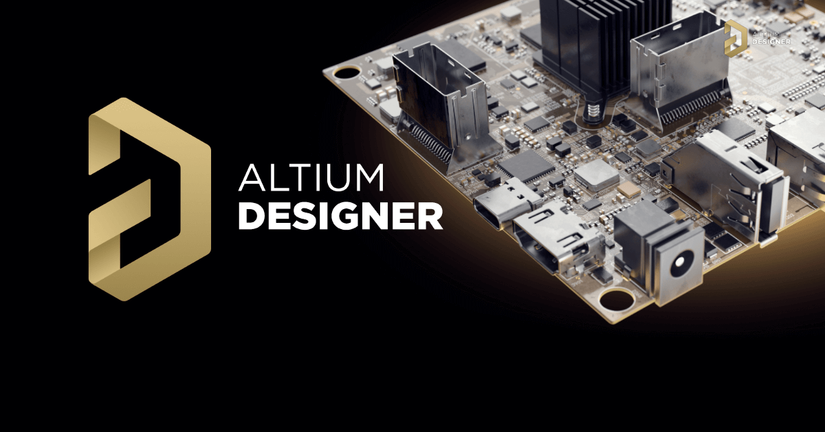
Altium Designer is a very good design software that belongs to the basic entry-level. It integrates techniques such as schematic design, circuit simulation, PCB drawing and editing, signal integrity analysis, and design output. It is very suitable for drawing a simple single board and double board and four or six-layer boards. For more design software issues, please refer to Top 9 Best PCB Design Software of 2020.
Step 2:Material preparation:
Some materials need to be prepared in advance before production, and the electronic components depend on the design drawing. Other required materials include
- Thermal transfer paper: Thermal transfer paper is required for subsequent thermal transfer processing. The thermal transfer process refers to printing various patterns on a special kind of paper with special thermal transfer ink, and then transfer the patterns to the product through temperature and pressure.
- Copper Clad Laminate (CCL): Different PCBs can be made by selectively processing on the copper-clad laminate.
- FeCl3: mainly used to remove the unnecessary copper layer on the copper clad board.
- Acetone: Mainly used to remove carbon transferred to CCL.
- Electric drill: used to drill holes on the copper-clad laminate.
- Sandpaper: used for polishing the surface of copper clad laminate.
- Beakers, tweezers, laser printers, irons, brushes,rosin water, Scissors, File , and other necessary auxiliary equipment;
Step 3:Production:
- 1. Printing: Here you need to use a laser printer to print the design drawing on the Thermal transfer paper, and finally get a black and white electronic circuit diagram.

- 2. Cutting: Cut Copper Clad Laminate (CCL) so that the size of Copper Clad Laminate (CCL) corresponds to the printed electronic circuit diagram, which is also the final product size.
- 3. Polishing:You can use sandpaper to polish Copper Clad Laminate (CCL) to make the surface of Copper Clad Laminate (CCL) rougher, and the processed PCB quality is better.
 4. Transfer process:This is a critical step, transfer the printed circuit drawings to Copper Clad Laminate (CCL). The specific method is to close the electronic circuit diagram to the CCL and then heat and press. You can use Iron Box or Heat transfer machine for heating and pressing. If you use Iron Box, you may need 10 minutes to complete the transfer process. It will be better to go with transfer machine or plastic packaging machine. Turn on the iron with higher temperature and start ironing on a solid platform. Stay the same direction when you iron and push as hard as you can. It is fine if there is little smoke during the whole process.
When the heat transfer is done. You can have a quick look about how the transfer goes when it is still hot. If it is perfect as you expect, you can just tear down the paper, or you can iron again.
 The CCL at this time has a conductive function but does not have an insulating function. Therefore, it is necessary to remove the unnecessary copper outside the CCL surface circuit to make it have the insulating ability.
- 5.Copper removal: FeCl3 solution is used here. Put the processed CCL into the FeCl3 solution to remove the copper in the non-circuit part of the CCL. The reason is that the following chemical reactions have occurred:
 The carbon in the circuit board does not react with FeCl3.

- 6.Decarbonization: The process of decarbonization is to remove the toner transferred on the CCL. When you decide to remove the carbon, put the CCL in the acetone solution , and gently brush off the toner with a brush. Or you can use physical methods such as sandpaper to remove the toner.

- 7.Drilling: Only when the holes are drilled correctly, the electronic components can be installed correctly. This step is relatively simple, just use an electric drill to drill a hole in the predetermined position of the CCL.
- 8.PCB Assembly: Install all electronic components in the correct position and solder them firmly.

Step 4:Test
The processed PCB needs to be tested to ensure that the board is in good condition. Turn on the power switch, the components are not damaged, and the circuit can achieve normal functions, it means that the PCB you made is good.
Tips
- When cut the material, make sure to clean the cooper on the edge of PCB or it will affect the final work of heat transfer
- When you have cleaned theCCL, do not touch the surface with your hand since it will affect the quality of the board.
- Make sure use plastic box for ferric trichloride, metal box is forbidden Here is the brief story for how to make pcb circuit board at home, it will be interesting for maker to have a try.
Advantages of DIY PCB:
The biggest advantage is that it can be manufactured quickly, and the finished PCB can be obtained in a short time;
Disadvantages of DIY PCB:
The manufacturing process is cumbersome, the efficiency is not high, mass production is difficult, and the quality cannot be guaranteed. It may not be possible for the average person to find all the materials. At this time, it is necessary to find a factory for processing.
Seeed Fusion PCB
Since it is affordable and easy to get PCB with free options of colors and beautiful silk-screen now, I have given up the home made PCB for a long time. Seeed Fusion PCB is affordable and quality guaranteed; Anyway, it still feel good to have a real my own PCB ( keep them in my collection). Enjoy yourself for the first try !If you want to learn more about DIY PCB, you can watch the video: