The Subtle Art Of Not Making Mistakes with PCB Design For Manufacturing

Getting your PCB design manufactured is no easy feat. Given the complexity of PCB design and manufacturing, there are plentiful chances for PCB failure to occur. Some of these failures can be a result of bad component placement and routing. If you arrange your components without consideration for the manufacturing process, chances are that you are going end up with a hideous board that doesn’t even work.
Fortunately, such a nightmare can be avoided. By understanding placement considerations and troubleshooting your designs on your own, you can make better placement and routing decisions to avoid unnecessary errors, and save lots of time and money on your next trip to your manufacturer. Having a strong foundation in board design can bolster your confidence in designing more complex boards for future projects. To help you create high-quality, manufacturable boards, here are ten basic PCB component placement and routing tips to consider when designing a PCB using design software.
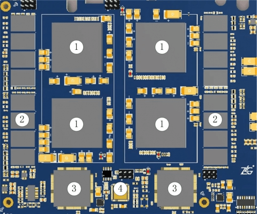
1. Place Larger Components First, Followed by Smaller Ones
Think of placing components as eating at a buffet. Given our limited stomach space, it is only natural that we go for the expensive or gourmet dishes first to make our money’s worth. Similarly, we would go about placing the important components first, before moving on to position the smaller ones.
(source: eefocus)
2. Orient Components in the Same Direction
Components should be oriented in the same direction, in either the X or Y direction, and arrange them neatly in rows and columns. This is to facilitate installation, inspection and reworking by you or your assembler. As much as possible, components with polarity requirements such as diodes, should be aligned such that all the positive poles are on one side and the negative poles on the other, with their polarity indicated on the silkscreen. Believe us, you’ll be thanking yourself later.
(Source: eefocus)
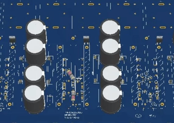
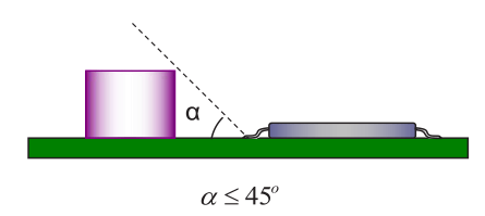
3. Avoid Placing Tall Components Next to Shorter Ones
Apart from the 2 dimensional arrangement, also always be mindful of the the height and width of the components. If taller components are blocking smaller ones, it may hinder inspection or maintenance and it is likely that solder joints will be poorly connected. You should maintain a viewing angle of no less than 45 degrees to aid manual solder joint inspection.
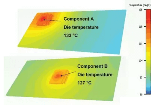
4. Place Heat Generating Components Near the Center of the Board
High current electronic components like microcontrollers can produce a lot of heat. Thus, it is a good idea to mount them near the middle of the board as this allows heat to diffuse throughout the board. On the other hand, if your component is mounted near the edge of the board, the heat generated can accumulate and the local temperature can get very high. In addition, if you have multiple heat producing components, space them out across the board to evenly distribute the heat throughout the board rather than having them cluster in one location. Improper heat distribution can cause your device to self-destruct, literally.
(Source: eefocus)
5. Keep Thermosensitive Components Away from Heat Producing Components
Likewise, it is best to keep heat-sensitive components such as resistive capacitors and thermocouples away from components big on releasing heat, such as resistors, diodes, inductors, rectifiers, MOSFETs and integrated circuits (ICs). For example, if capacitors get too hot, they will begin to lose their ability to retain charge, shortening the lifetime of the device.
Besides providing electrical connectivity between layers, did you know that vias can also be used to dissipate heat from one side of the PCB to the other? To lower the operating temperature of super-powered components like ICs, vias can be placed below the IC to channel the heat away.
6. For Components Using Wave Soldering, Align them to the Direction of the Wave
In ware soldering, surface mount devices (SMD) are usually attached to the bottom of the board with adhesives and then passed through the molten solder. If you are going to have your design wave soldered, your parts should be orientated in the direction parallel to the direction of the wave to prevent solder shorts or open connections. For instance, if you have a small component behind a tall one in a defect-prone orientation, it might create shadow effect problems, resulting in the smaller component having insufficient solder or none at all.
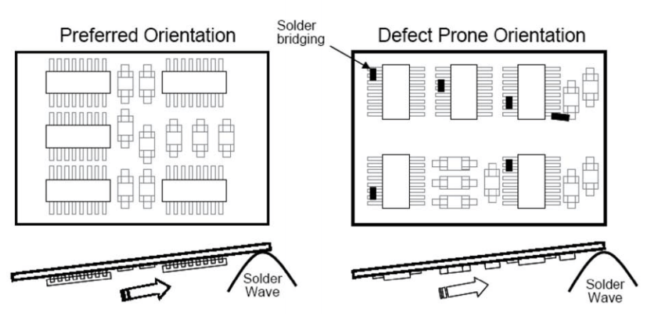
Preferred orientation with components parallel to the direction of the wave (left), vs a defect-prone orientation with shadow effect problems (right)
(Source: SMT Magazine)
7. Don’t Use Sharp 90 Degree Trace Angles
When you have traces that have a sharp right angle turns, there is a risk that the outer corner of the 90 degree angle will be etched narrower than your standard trace width. In the worse case scenario, your board might return to you with 90 degree traces that are not fully etched, which might lead to short circuits. Also, another reason why engineers avoid right-angle traces is due to the possibility of high speed logic signals being reflected off the back of the right angle, causing interference.
A solution is to use 45 degree angle traces. Not only does it makes everyone’s life easier, but it also shortens the electrical path between components compared to 90 degree angles. What’s more, 45 degree angle traces are known to produce beautiful PCB layouts!
8. Keep Connections as Direct and Short as Possible
The goal is to keep compatible parts grouped together in the same area to minimize the length and crossing of airwire connections between your components. This is beacause long traces can pick up electromagnetic noise from other sources and potentially lead to interference.
9. Increase the Width of the Power and Ground Traces
With more current flowing through them compared to other traces, the power and ground traces are more prone to being burned up if they are kept skinny like the rest. By making them wider, you can reduce the heat generated and prevent your board from being ruined.
But keep in mind that the width of your traces is also determined by the proximity of the traces to components and adjacent traces. If you are squeezing lots of components and traces into a small PCB, then the traces have to be narrow to fit everything.
10. Perform a Design Rule Check (DRC)
Using DRC to check that your design is error-free is a great habit to adopt as you go along designing your PCB. Using the DRC will help you to identify problematic designs, enabling you to correct potential manufacturing issues that could result in low manufacturing yields. You can avoid unnecessary costs that would otherwise be incurred from manufacturing errors and delays in product releases.
If you have already grasped the basics and found this a naggy and boring read (congrats on getting this far), Seeed’s very own PCB Design for Manufacture guide might just be the guide that you were looking for. To help bridge the gulf between design and manufacture and help people ensure that their design is manufacturable, we have penned down a detailed design for manufacture guide on the component layout, fiducial design, trace design, solder mask layout, silkscreen considerations among many other design parameters. We have condensed our 10 years of manufacturing experience into this manual, and are still continuously improving it to better serve the community.
Already have your PCB design ready for manufacturing? The Seeed Fusion PCB Manufacturing service is capable of fabricating the simplest of boards to the most complex designs, for large scale production down to a single board. And if you don’t fancy putting the device together yourself, try the Seeed Fusion PCB Assembly service. With an intelligent BOM reader and direct access to livestock pricing data from renowned component distributors like DigiKey and Mouser, the Seeed Fusion online platform is able to instantly provide you with complete quotes up front within a matter of seconds. You can also preview your design with the Gerber Viewer before submitting them. Find out how you can translate your designs into reality here.
If you have more detailed inquiries or questions about DFM, welcome to communicate directly with our manufacturing experts on our Forum.