PCB Panelisation Tips for Assembly

Printed circuit boards can come in all shapes and sizes, which presents various challenges to board designers when constructing the panel layout. To illustrate the range of issues possible, we present 3 different cases where poor panelization resulted in production difficulties at Seeed’s assembly facilities and the subsequent solutions.
Panelizing a design has multiple benefits and in some cases is mandatory for automated assembly. Connecting multiple copies of a small board to make a larger panel may be necessary to satisfy the equipment’s minimum size requirements or make handling easier. But it also reduces the production cycles needed, thereby greatly reducing the assembly time.
For automated assembly, the PCB panels require tooling margins, which serve as the rails that allow them to travel on the conveyers from machine to machine. Without these rails, it would be difficult to control the alignment of the boards and hold them into place. The margins also ensure that all parts of the individual board are accessible on both sides during assembly.
Aside from the size and geometry of the individual board, other factors such as component layout, panel strength, depanelization procedure and individual PCB features must also be taken into account. In our first case, for example, the partial overlap of the audio jack and the micro-USB connector were not considered, making it impossible to have them both assembled at the same time.
To work around this issue, the audio jack was omitted from the first reflow step, the boards were depanelized and then the audio jack was populated manually. While the technicians were able to meet the deadline for this project, the extra effort could have been avoided at the design stage.
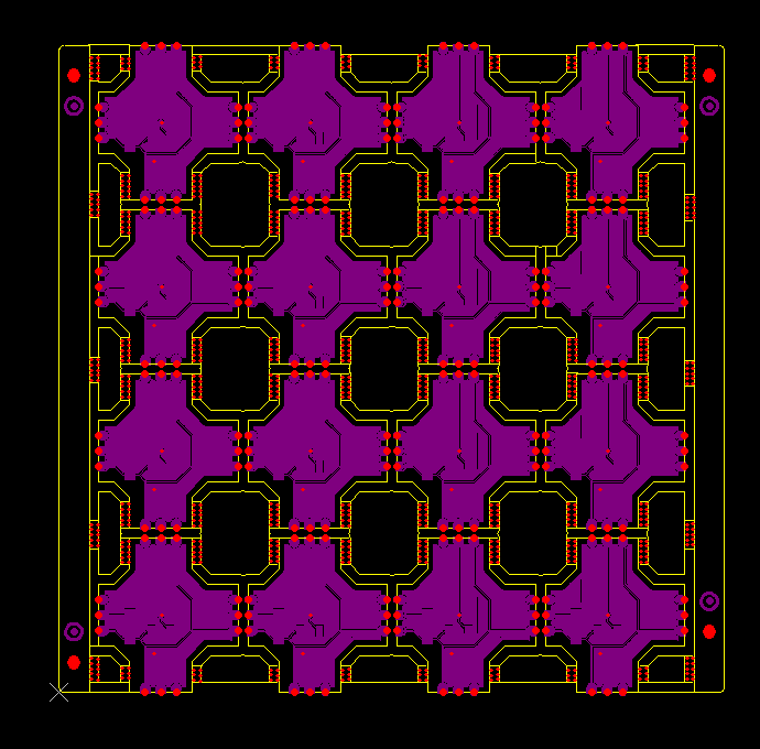
Usually, overhanging components should not cross a v-cut as this would obstruct the depaneling blade used to split the boards from the panel post assembly. But for this particular design, there was an added complication in that both top and bottom sides are lined with gold contacts. These should also have a clean routed edge to aid insertion into a connector. Therefore, it is not possible to simply rotate the boards and have the v-score cut along these edges. A little creativity and compromise was required, resulting in the design below:
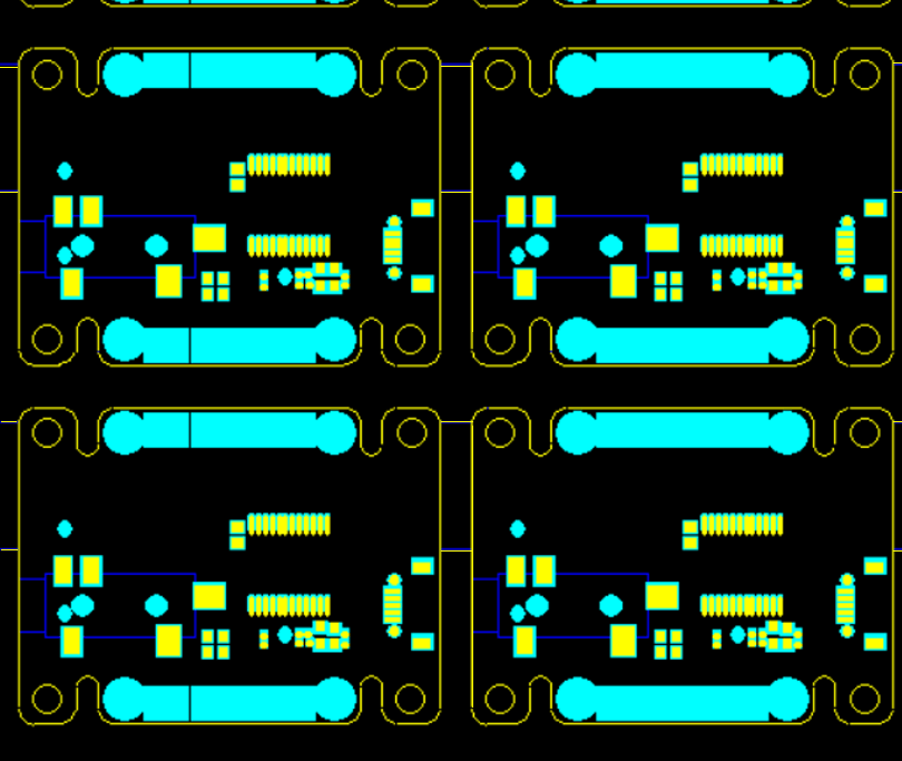
Notice the strategically placed tabs holding the boards apart while maintaining as much panel strength as possible. Although technicians would have to remove each of these tabs manually, this is much quicker and less labor-intensive than having to solder the audio jacks one by one.
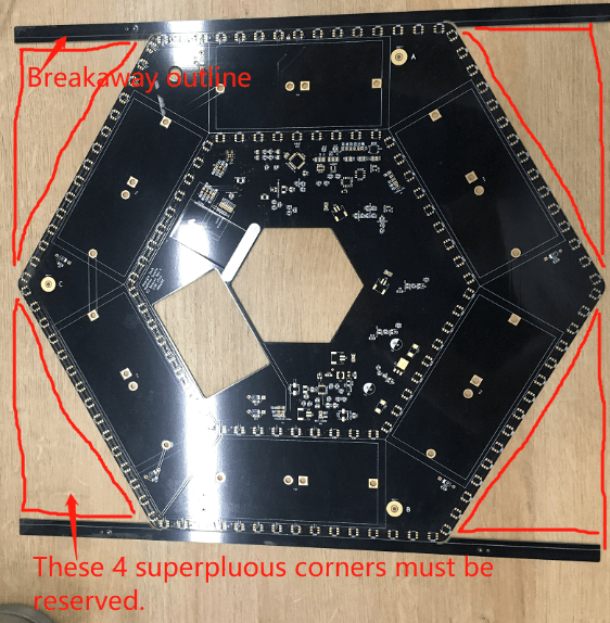
In another case, to make the panel, tooling margins were simply added to the top and bottom sides of these large hexagonal boards. However, during assembly, the engineers discovered that the pick and place machines’ position hammer could not register the position of the board accurately, or failed to register the presence of the board at all.
The lack of PCB material on the front edge of the panel meant that stop hammer would impact an angled edge, thereby stopping the panels at slightly different points along the direction of travel. This variation made it difficult for the pick and place camera to locate the fiducials on the board and position it accurately.
In fittingly maker fashion, pieces of excess material were attached to the front end of the panel to provide a straight perpendicular edge for the hammer. Future panel designs replaced the corner material by connecting them using perforated tabs.
In the third and final case, a 3×4 panel of Grove 2-Channel SPDT relay module boards was constructed. However, the large size and weight of the relays caused the panel to sink and bend towards the middle. During reflow and selective wave soldering, joint defects and board warping weres observed.
At the time, tweaking the wave soldering machine’s program helped to alleviate some of the issues but the quality fail rate was still high. Subsequently, many defective pieces had to be re-worked manually.
In future runs, the panel was reduced to a 2×4 layout, small enough for the panel to withstand the weight of the relays without deformation.
The three different cases go to show the sheer range of possible problems arising from the least expected places that go beyond PCB Design for Manufacture. From component layout, equipment capability to the physics of the loaded panel, the designer must understand and consider not just software and hardware but also manufacture and assembly. The latter part we like to call Design for Assembly – expertise which is pooled up by Agile manufacturers such as Seeed.
So how can designers avoid such costly mistakes? While there are no foolproof set of guidelines, it is helpful to keep in mind a few select points when considering a panel design.
- Board Shape: As a general rule, panels should be rectangular and symmetrical as much as possible. Otherwise, the imbalance and dissymmetry may introduce areas of weakness in the panel and cause warping or concentrate stress in weak areas.
- Board Size: For size, it is recommended that a panel size greater than 50 x 50mm and less than 280 x 280 mm be adopted. Minimum and maximum sizes vary from machine to machine but maintaining dimensions within this range ensures compatibility with most assembly lines and just makes the boards easier to handle during production. Where components are particularly heavy or inter-board connections are weak, smaller panels are better.
- Tooling Margins: A tooling margin width of at least 5mm on at least two opposite sides (preferably along the longest sides) is recommended for easier handling and greater panel strength. Typically, panel fiducials are added to three corners of the panel on the tooling margins for machine registration.
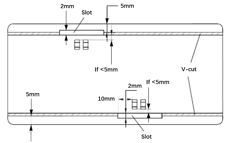
- Component Placement: V-cuts and stamp holes/tabs should not be added close to components. The stress applied to the boards during depaneling can easily fracture the component or the solder joint. Especially fragile components like ceramic capacitors, within 5 mm of the board edge should have special care. A milling slot can be introduced directly beside the component if using v-cuts to avoid high-stress points.
- The depaneling method: The method adopted to break apart the boards after assembly also plays a key role in early design decisions. V-cuts? Tabs and stamp holes? Manually? Automated? If using a depaneling machine for example, the boards should be spaced apart and laid out in such a way that the blade can easily pass without hitting obstacles. Panels must also be designed to allow the panel to be easily dismantled after assembly.
- If de-paneling by hand, v-cuts and stamp holes/tabs should not be added close to components since the stress applied to the boards during bending can easily fracture the component or the solder joint. Especially fragile components like ceramic capacitors should be at least 5mm away from the v-cut or tab.
- PCB manufacturing considerations: A notable example: to make castellated holes or plated half holes, the holes need to either be on the outer edges of the panel (for dip plating processes), or routed (for routed half holes). This often means that these edges are reserved and cannot have v-cuts or tabs across them, thus may strongly influence the design of the panel. Some people may say that a square board with castellated half holes on all four sides cannot be panelized, but a little creativity suggests otherwise.