Analog to digital converter——ADS1015
ADS1015 is an AD conversion chip produced by TI. It adopts IIC serial protocol communication, 4 conversion channels, 12-bit conversion accuracy, maximum conversion speed of 3.3ksps, built-in gain amplifier, users can set the gain according to their needs. The same series as ADS1015 also has ADS1016, 16-bit conversion accuracy.
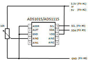
In addition, AIN0 and AIN1 can be used for differential measurement with AIN3. Configure the multiplexer in MUX[2:0 of the configuration register. ]
When measuring a single-ended signal, the negative input of the ADC is internally connected to GND through a switch in the multiplexer.
ADS101x uses a switched capacitor to continuously charge and discharge the capacitor in the input stage to measure the voltage between AINP and AINN. The ADS101x has a 1-MHz internal oscillator, which is divided by 4 to produce an fMOD of 250 kHz. The capacitance used in this input stage is very small, and the average load is resistive to the external circuit. Figure 11 shows this structure. The capacitance value sets the resistance and switching rate.
During the sampling phase, switch S1 is closed. This allows CA1 to V(AINP), CA2 to V(AINN), CB to (V(AINP)-V(AINN)). In the discharge phase, S1 is first opened, and then S2 is closed. Then CA1 and CA2 are discharged to approximately 0.7 V, and CB is discharged to 0 V. This charging will draw a very small transient current from the power supply driving the analog input of the ADS101x.
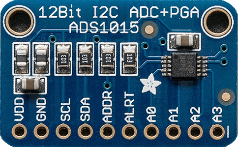
Pin introduction of ADS1015
1. ADDR address pin (connect to different pins to set different addresses, the address of the GND pin is 0x48)
2. ALERT interrupt pin, voltage comparison can be configured in the chip, which can be used as a numerical comparator output or conversion ready pin
3.GND ground wire
4.AIN0 AD conversion channel 0
5.AIN1 AD conversion channel 1
6.AIN2 AD conversion channel 2
7.AIN3 AD conversion channel 3
8. Connect VDD to 2.0-5.5V
9. SDA IIC data cable
10.SCL IIC clock line
The pins can set different addresses according to the four pins connected to GND, VDD, SDA, SCL, as shown in the following table:
| ADDR PIN | SLAVE ADDRESS |
| Ground | 1001000 |
| VDD | 1001001 |
| SDA | 1001010 |
| SCL | 1001011 |
Register of ADS1015
ADS1015 has four registers, as shown in the figure below, BIT1 and BIT0 represent the address of the register, corresponding to the conversion register, configuration register, low threshold register and high threshold register respectively. Among them, the conversion register stores the result of AD conversion. Since the conversion result is 12 bits, the data should be shifted to the left by 4 bits when reading, the register is configured to configure the chip parameters, and the high threshold and low threshold registers are used as voltage comparison functions.
| BIT1 | BIT0 | REGISTER |
| 0 | 0 | Conversion register |
| 0 | 1 | Config register |
| 1 | 0 | Lo_thresh register |
| 1 | 1 | Hi_thresh register |
Register related configuration
The configuration register is needed to configure the ADS1015 chip, as shown in the following table:
| BIT | 15 | 14 | 13 | 12 | 11 | 10 | 9 | 8 |
| NAME | OS | MUX2 | MUX1 | MUX0 | PGA2 | PGA1 | PGA0 | MODE |
| BIT | 7 | 6 | 5 | 4 | 3 | 2 | 1 | 0 |
| NAME | DR2 | DR1 | DR0 | COMP_MODE | COMP_POL | COMP_LAT | COMP_QUE1 | COMP_QUE0 |
Several important register configurations:
(1) BIT[15] OS bit: This is to set the mode of chip data reading, whether it is single reading or continuous reading.
(2)BITS[10-11]: Configure voltage gain.
(3)BITS[7-5]: Configure the conversion speed.
I2C interface
ADS101x communicates via I2C interface. I2C is a two-wire open-drain communication interface that supports multiple devices and hosts on the same bus. Devices can drive the bus only by pulling the bus low by themselves, and cannot drive the bus when the bus is high. Therefore, the bus requires a pull-up resistor, so when there is no device driving the bus, the bus is always high. In this way, there is no conflict. If two devices drive the bus at the same time, there is no drive contention. Communication on the bus always takes place between two devices, one as the master and the other as the slave. Both the master and the slave can read and write, but the slave can only read and write under the request of the master. So I2C devices can be used as master or slave, but ADS101x can only be used as slave.
An I2C bus contains two lines: SDA and SCL. SDA transmits data; SCL provides clock. All data transmitted through I2C is a group of 8 bits. When SCL is low, drive the SDA line to send data to the I2C bus (low level means 0, high level means 1). After the SDA line data is prepared, the SCL line is pulled high and then pulled low. Through such pulses, SDA puts the data in the shift register. If the bus remains idle for more than 25ms, the bus will time out.
The I2C bus is bidirectional, that is, the SDA line both receives and sends data. When the host reads data from the slave, the slave drives the data line, and when the host sends data to the slave, the host drives the data line. The clock line is always driven by the host. ADS101x cannot be used as a host, so it cannot drive the SCL clock line. When communication occurs, the bus starts to change. Only the host can start a communication and establish a start condition. Under normal circumstances, the data line changes state only when the clock line is low. If the data line changes state when the clock line is high, it means another communication start or end condition. The establishment of the start condition requires that when the clock line is high, the data line changes from high to low.
The establishment of the end condition requires that when the clock line is high, the data line changes from low to high.
After establishing a start condition, the host needs to send a byte to indicate which device to communicate with. This byte is called the address byte. Each device on the I2C bus has a unique 7-bit address to respond. The host sends a bit along with the address byte to indicate whether it needs to be read or written. Every byte (address or data) sent on the bus will be acknowledged by an acknowledge bit. After the master sends a byte (8 bits) to the slave, the master releases the data line and waits for the response from the slave. The response of the slave is indicated by pulling down the data line. The host then continues to send clock pulses to record this response. Similarly, when the host finishes reading a byte, the host pulls down the data line to indicate a response to the slave. The host continues to send clock pulses to record this response. The clock line is always driven by the host.
If the host tries to communicate with a device that is not on the bus, it will receive a non-response, because there is no device at that address to pull down the data line to answer the host. The non-response performance is as long as the data line is kept high during the response period.
When the master and slave end communication, an end condition needs to be established. When the end condition is established, the bus resumes the idle state. At this time, the host can establish another start condition. Establishing a start condition when the bus is in use is called repeated start.
The development of a product is inseparable from PCB assembly. In order to make the product performance more reliable. For more details about the product ADS1015, please click Seeed Fusion.