Are my PCBs Single or Double-Layered? Seeed Fusion PCB Know-how
With everyone resorting to learning online, there’s no better time to share knowledge freely on the wide worldwide web. So, we thought we’d share some practical and up-to-date PCB manufacturing know-how based on real problems and questions we encounter. Today we start with a common but rather unexpected dilemma that often catches our customers by surprise.
Disclaimer: Please note that this knowledge is based on the Chinese PCB industry, mainly small to medium batch quick-turn PCB manufacture, but we aim to be as general as possible. Some nuances and differences in opinion may exist.
How many layers does my PCB have?
At first glance, this should be an easy question to answer. 4-layer, 12-layer, 32-layer PCBs are commonplace and easy to understand – the number just refers to the number of copper layers right?
Yes, but when it comes to single, double, or even zero-layer PCBs, you might be forced to stop and think before filling in that PCB order form. Is my PCB single or double-layered? Why is there so much confusion? I chose single-layer but my files are actually double-sided – will they only make single-layer PCBs? Does it really matter? In this article, we try to tackle these points.
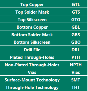
Let’s start with some definitions. Traditionally, the number of layers of a board refers to the number of copper layers, specifically, the number of layers with copper traces or pour – just having pads does not count, partly as a safeguard if the design software fails to export the traces or pour for whatever reason.
So what is a single-layer board?
SMT Single-Layer board
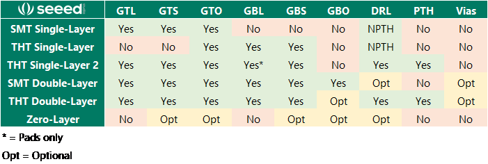
The simplest type to understand is the surface-mount single-layer PCB board. This is what you’d expect – traces and pads covered by solder mask and then overlaid with silkscreen printing. There shouldn’t be anything on the other side. No plated through-holes or vias.
GTL, GTS and GTO -> more common
or
GBL, GBS and GBO
THT Single-Layer board
This is where things get a little complicated. Beginners often forget that a through-hole single-layer board typically needs the silkscreen on the other side of the solder pads.
GBL, GBS and GTO -> more common
or
GTL, GTS and GBO
The silkscreen typically contains information on the component outline, polarity markers and designators/values. The side with the silkscreen printing is the side where the body of the component lies. The leads are inserted through the through-holes and soldered to the pads on the opposite side.
Also a THT Single-Layer board
The traditional definition does not count copper layers which only contain solder pads as contributing to the layer count. So technically, a single-layer board can also have plated-through holes, so long as one of the sides only contains pads in the copper layer.
GBL (pads only), GBS, GTO, GTL and GTS
or
GTL (pads only), GTS, GBO, GBL and GBS
Plated through-holes, No vias
Which side the traces are on is functionally irrelevant since they are electrically connected via the through-holes, but having them on the side with the silkscreen should help with inspection and trouble-shooting. This combination could also support mixed assembly (THT and SMT) if the surface mount components are placed on the side with the traces.
Some fab houses may not like this combination and may ask you to confirm how to proceed,
SMT Double-Layer boards
This board is typically the same as the single-layer surface mount except surface mount parts are on both sides. If the two sides form a single circuit, vias are needed to pass the signal through the substrate.
THT Double-Layer boards
Traces on both copper layers, solder mask on both sides. Can have mixed assembly. Nothing too difficult to understand. Signals can be transmitted between sides through plated through-holes or vias.
Zero-layer boards
A very special case driven by the increased accessibility of PCB manufacture. A zero-layer board is essentially a board with no copper – it is not designed to be electronically functional but may have solder mask or silkscreen. We sometimes see these when people use our service to make washers, business cards, or customized panel covers for example. This is not common practice, so you will rarely see the option to choose zero-layer boards on any online form.
So that covers most of the oddly defined combinations. Within these, there are other possibilities, but we’ve listed the most common combinations in the table below.
Why is there so much confusion?
In my experience, I think the problem is due to different definitions and the lack of specificity. There is no complete definition that clears up the misunderstandings. For example, manufacturers and industry experts often use the terms single-sided and double-sided synonymously with the terms single-layered and double-layered. If we said this is a 4-layer PCB then there is no confusion, but 4 sided doesn’t make sense. So, ‘sided’ should refer to the top and bottom sides of the PCB, regardless of what is in the middle. Following that logic, a 4-layered PCB is also a double-sided PCB. Notice that we’ve been careful not to say single or double-sided in the article.
Assembly Types
As seem, another way of defining a PCB is whether it is for single-sided or double-sided assembly. This information is of little importance to a board manufacturer but could add another element of confusion into the conversation.
Exceptions
Certain combinations of Gerber layers may form an exception to the standard definitions. From the definition of copper layers, it clearly doesn’t care about the solder mask or silkscreen or even pads. So, to fully define a board you may have something like:
Double-layer boards
Double-sided pads
Double-sided solder mask
Single-sided silkscreen
(for the third example in the table)
With more and more PCB designs that have aesthetics in mind, the lack of solder mask on one side could mean the difference between a quality board and a cheap product. But how do you communicate this in the Gerber files and order parameters?
If you like dismantling consumer products, you may have come across single layer PCBs that do not have solder mask on one side, which is designed to save on production costs. But when was the last time you saw a development board or module on the market with substrate showing through?
Some PCB software is to blame
Every now and then we see Gerber files sharing similar traits and similar problems. One of those problems is outputting double-layer boards with what seems to be plated through holes but only with pads on one side. There are already two copper layers, so why not make these plated holes? Having plated through-holes would allow you to apply more solder to the joint and strengthen the bond.
Some Smart Gerber viewers encourage a change of definition
An increasing number of customers and manufacturers rely on smart Gerber Viewers to automatically detect the layer count of a board and then flag it if there is a discrepancy. How do they do that? Basically, they just count the number of Gerber files named as copper layers. But most can’t tell what is inside the file. So users who rely heavily on these, are tempted to simplify the problem by changing the definition.
Double and Single-sided boards. Does it matter?
Perhaps this should have been the first question since, for 99% of designers, the answer is no. No, you haven’t just wasted 10 minutes reading something completely useless.
Yes and no. It depends on the size of production. For mass production, every consideration should be made into where costs can be minimized. If that means single-sided boards then sure, go for it. If you are just at the prototype stage or going for a small batch, then whether a board is single-sided or not is irrelevant in terms of costs and quite frankly, just complicates things.
It does not cost more to produce double-layer boards
It may even involve more work. Double-layer boards are by far much more common than single-layer boards. So manufacturers keep big stocks of cores – FR4 substrate covered on both sides with copper. To make a single layer board, all the copper on one side has to be etched away.
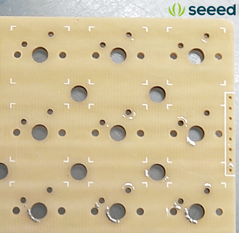
If too much copper needs to be removed on a panel then the etching solution and etching time may not be sufficient to remove all the copper. In the image above, note the remnants of copper which have been plated with silver HASL surface finish left on the edge of some of the drill holes.
Despite that, single-layer boards typically don’t cost extra. In fact, at Seeed Fusion, we’ve even considered removing the single-layer option entirely – how many people specifically do NOT want pretty protective solder mask on both sides anyway? The reverse situation is more likely (single-layer boards, double-sided solder mask). Your thoughts? Let us know in the comments section and maybe we will actually do it.
Final question: I chose single-layer but my files are actually double-sided – will they only make single-layer PCBs?
Most fabs won’t be that drastic and will either ask you to confirm or just follow the files. Another reason why the single layer option doesn’t really matter much.
Congrats on getting through this somewhat long-winded article. We hope it gives you a little insight into the manufacturer’s perspective when it comes to interpreting clients’ intentions. We’ll be bringing more soon!
Yes, very nice.
Perhaps in a follow-up article you can cover Surface Treatment, double drilling, panel test.
Different material, FR4, aluminium, HDI, copper base (maybe you covered this already)
Surface finish, maybe samples of different solder masks, colors.
Interesting topics !!
Thank you!
Oh yes, this is just the beginning – there is a wealth of information to work with. Thank you for the suggestions!
Great job Carmen. A very well written and informative article. Thanks!
Thank you! I thought I’d try another approach compared to the gazillion generic single vs double vs multi-layer PCB articles out there. Glad you liked it.