PCBA Quality Control: Flying Probe, AOI, X-Ray, ICT and FCT Explained

A board goes through several checks and tests as it moves from a bare PCB to a finished assembly. The reason is simple: each method checks something different—whether the traces are connected, whether components are placed correctly, whether hidden solder joints are sound, or whether the assembled board works when powered. No single method covers them all.
If these defects remain undetected until final assembly or reach the customer, rework and troubleshooting become much more costly. PCBA quality is built by catching defects at each stage of production.
This article covers the five inspection and test methods Fusion commonly uses in PCBA production—flying probe, AOI, X-ray, ICT, and functional test (FCT)—what each one finds, and how they work together to reduce the risk of defects reaching the customer.
📋 The five methods at a glance
| Method | What it checks | What it finds |
| Flying probe | Traces on the bare PCB | Opens, shorts, and other trace faults |
| AOI (with manual review) | Component placement and visible joints | Missing or misaligned components, reversed polarity, tombstoning, solder bridges, and solder anomalies |
| X-ray | Hidden solder joints under BGA and similar packages | Voids, bridging, insufficient solder, opens, and misalignment |
| ICT | Electrical connections and component values on the assembled board | Opens, shorts, incorrect component values, or reversed polarity |
| Functional test (FCT) | Functions specified in the Test Plan | Failures involving power, interfaces, firmware, and other functions covered by the Test Plan |
Each is introduced below in production order. Which of them a given board goes through depends on its design, its components, and your requirements—not every board runs all five.
📍 Flying probe: verifying the bare board’s traces
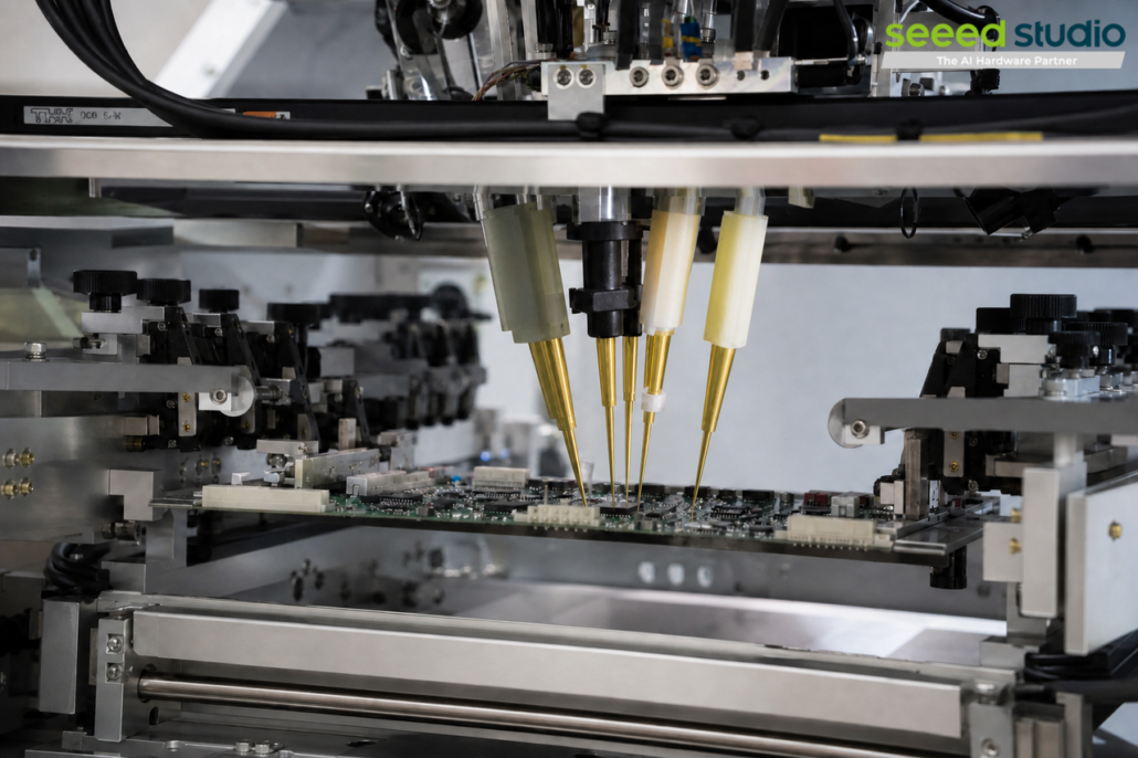
Before component assembly, the bare board’s traces are checked. Flying probe uses probes that contact test points one at a time to check the traces for opens and shorts. It requires no custom bed-of-nails fixture, making it suitable for prototypes and high-mix, low-volume production.
Checking the traces before assembly avoids wasting components and labor on a board that already has a broken connection.
📐 AOI: checking component placement and soldering
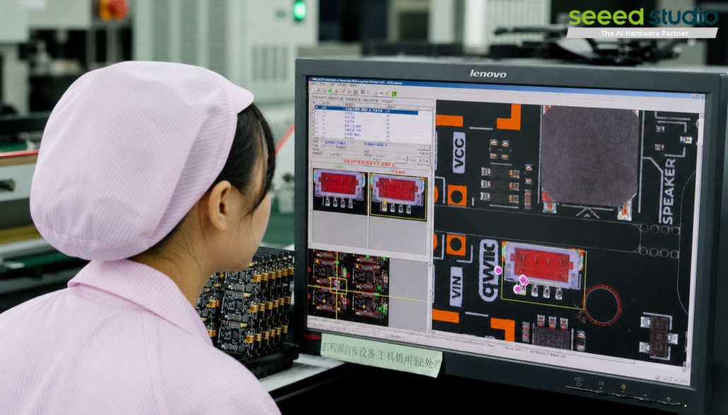
After placement and reflow, AOI checks component placement and soldering. It captures images of the board and compares them with predefined criteria to flag missing or misaligned components, reversed polarity, tombstoning, solder bridges, and insufficient solder.
AOI speeds up inspection by screening the board for anomalies. Operators review the flagged results and perform additional visual checks where needed. This helps catch visible placement and soldering defects before the board moves to the next stage. AOI can inspect visible solder joints; hidden joints may require X-ray.
🛠️ X-ray: checking the joints you can’t see
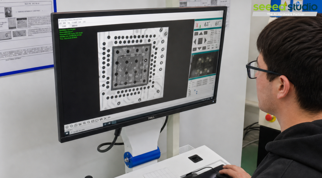
When the board contains BGA or similar packages, the solder joints sit beneath the components, where neither AOI nor visual inspection can see them. X-ray reveals these hidden joints and checks for voids, bridging, insufficient solder, opens, or misalignment.
It helps catch hidden-joint defects before shipment, reducing the risk of problems appearing during final assembly or in the field.
🛠️ ICT: checking the assembled board’s electrical connections
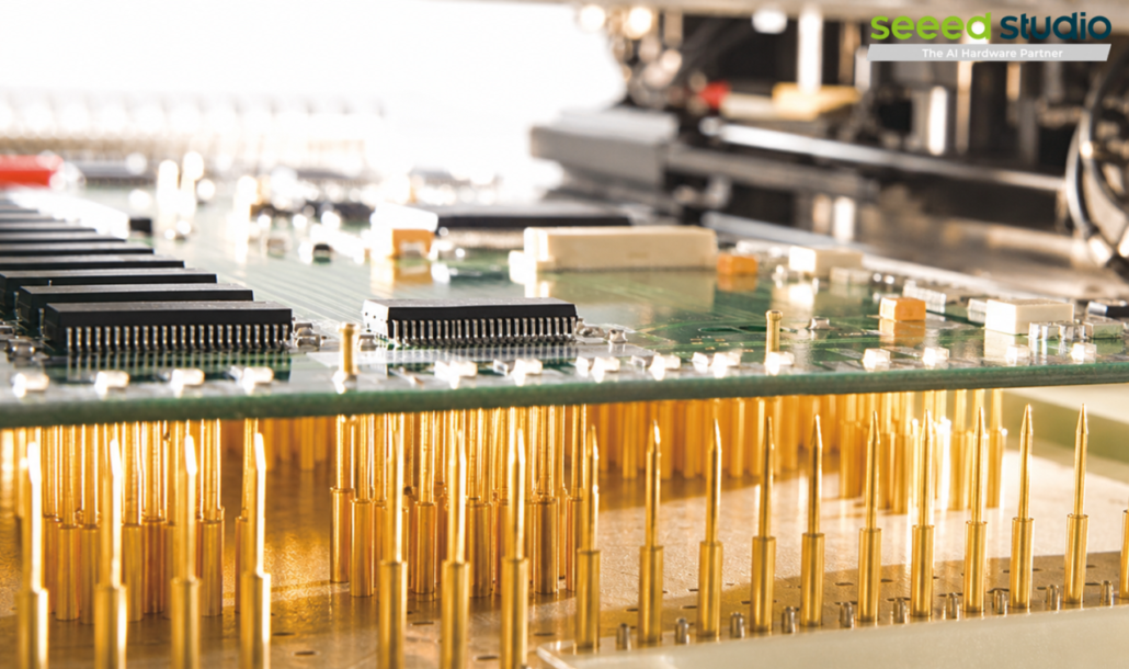
Unlike flying probe on the bare board, ICT checks the fully assembled board. After assembly, ICT uses a test fixture to contact the board’s test points and check for opens, shorts, incorrect component values, or reversed polarity.
ICT is well suited to stable designs in repeat production, allowing electrical connections to be checked quickly and consistently across a batch.
🛠️ Functional test (FCT): verifying the board actually works
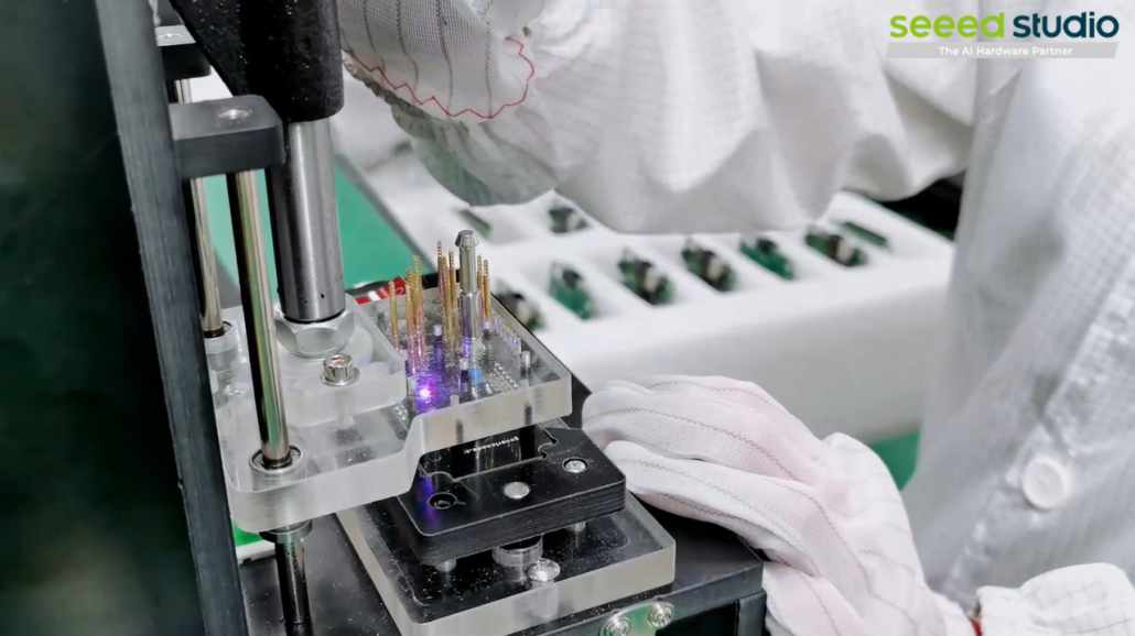
The methods above check assembly and electrical connections. FCT powers the board and checks whether the functions defined in your Test Plan work as expected.
Because each product has different functions and pass/fail criteria, functional testing requires a customer-provided Test Plan. Without one, functional testing is not performed by default.
Fusion offers free functional testing. To request it, upload your Test Plan on the order page (a Test Plan Example is provided; ZIP/RAR, 20MB max). If it is not ready, choose “add test plan later” and upload it in the cart.
📐 Common questions
Does every PCBA go through all five checks?
No. The checks applied depend on the board design and production requirements—hidden joints under BGA may require X-ray, and functional testing needs a Test Plan from the customer.
Is functional testing still needed after AOI?
AOI checks soldering and placement, while functional testing checks the board functions covered by the Test Plan. Whether FCT is needed depends on your product and testing requirements. The two methods identify different types of problems.
When is X-ray used?
X-ray may be used when the board has BGA or similar packages whose joints sit beneath the components. It checks for voids, bridging, insufficient solder, and opens.
Does functional testing cost extra, and how do I request it?
Fusion offers free functional testing when you upload a Test Plan; without one, it is not performed by default. If a new test program, dedicated fixture, or special setup is required, the team will confirm the details with you before production.
✅ Want to verify the whole unit? Upload your test plan with the order
These five methods cover different stages of production—from bare-board traces and component placement to hidden solder joints and the board functions covered by the Test Plan—helping reduce the risk of quality issues reaching the customer.
When you submit a project, provide complete Gerber, BOM, and assembly files; identify any components in BGA or other packages that require special attention; and if you require functional testing, include your Test Plan and related test files.
For functional testing or special requirements: upload your Test Plan on the order page or contact [email protected]. We will reply within two business days.
Upload your Gerber and BOM for a quote👉: Fusion PCB/PCBA order page
About Author
