Making Christmassy PCB art with Inkscape, SVG2Shenzhen and KiCad

Ever wanted to “draw” a PCB? In this article, I attempt to draw and manufacture a pretty PCB from scratch in just one week using Inkscape, KiCad, Seeed Fusion service and a nifty Open-Source Inkscape extension, SVG2SZ. Check out how it went (failed) here.
A little background..
A couple of months ago, the big boss approached a colleague and me about a visitor who had some special PCB requirements. He handed us a sample of the red PCB and told us they would be coming for a talk a while later. Such a direct request doesn’t come every day so, to prepare, we inspected the boards, followed the link in the silkscreen and checked out the YouTube videos and anything else we could find.
The specifics aside (we couldn’t get our heads around the science), we were satisfied that we’d done enough research for our little discussion and the scheduled time soon came. The visitor, Marc, arrived with a companion and began by showing us some spectacularly artistic PCB designs, nothing like the one we had spent the last hour researching. Each PCB appeared as if each layer was hand drawn, by hand or using graphics design software, not like what could easily be achieved in standard PCB design packages. Some had wavy flowing traces, fun bold copper text and accents, and on some designs, you could barely tell that these were fully functional PCBs that were meant to be populated.
Now, over the course of working in Seeed Fusion, I have seen and reviewed the Gerber files of close to 10,000 PCB different designs. Every now and then some interesting PCB art comes up, but nothing like the designs Marc had brought over. My colleague and I were pleasantly surprised but confused. What had this got to do with the red sample we were given? Marc then swiftly replied along the lines of, oh, that’s not my design. It’s my friend’s (who is not here). I didn’t come to talk about that. He then proceeded to tell us about an extension that was used to make these designs possible. And he was on a mission to spread the word.
Indeed, I had heard of the popular Eagle ULP, “import.bmp,” and used it to add simple graphics to PCBs. But it is fiddly, and if used for elaborate PCB designs, it can produce humongous files that either crashed Gerber viewers or exceeded online fab houses’ upload limits (though this problem appears to have been resolved in the latest Eagle update).
This new approach is designed specifically for KiCad, using the popular and free vector graphics editor Inkscape. In brief, it involves drawing the PCB design by hand, scanning it into Inkscape and creating each of the layers. Then, by using the Inkscape extension, the layers can be exported directly as a KiCad PCB file or even a footprint module.
Curious, I thought I’d try it out for myself. I had always admired the creative (but somewhat crazy) designs of DEFCON badges and often find myself pausing for a moment to appreciate our customers’ more elaborate designs. So, what better time to make a flashy PCB than now, when it just doesn’t feel festive without some colorful sparkle.
So, with Christmas around the corner, I set myself a challenge: Could an electronics novice with no PCB design experience, design and manufacture a PCB in one week?
Ok, to be completely honest, I am not a complete novice. Yes, I have never designed a PCB before and the last time I used Ohm’s law was in high school, but from working with PCB manufacturers and designers, you could say I have a reverse engineered understanding of PCB design. There are advantages and disadvantages, but for this task, I felt confident.
Next point, yes, as you may have guessed, the result was not what I had originally intended. At the beginning, I wanted to have a fully working, flashing, LED badge complete with 555 timer, a pair of tiny 0603 LEDs soldered upside-down on the back of the PCB so the light would only be visible through a little drill hole, using all Seeed OPL components (i.e., raid the warehouse), hand soldered and.. you get the point. Call me ambitious.
For simplicity sake, I will just describe the basic workflow from getting from design to manufactured board. To do this yourself, you are going to need KiCad, Inkscape, the extension, and a chosen PCB manufacturer. A bit of creativity would help too.
Please note though that the advice and considerations made in this article are from my own experience with Seeed Fusion. Other, especially non-Chinese manufacturers may have different rules and approaches. Please ask your manufacturer for more advice if in doubt.
Without further ado, let’s begin!
Task 1: Come up with a design
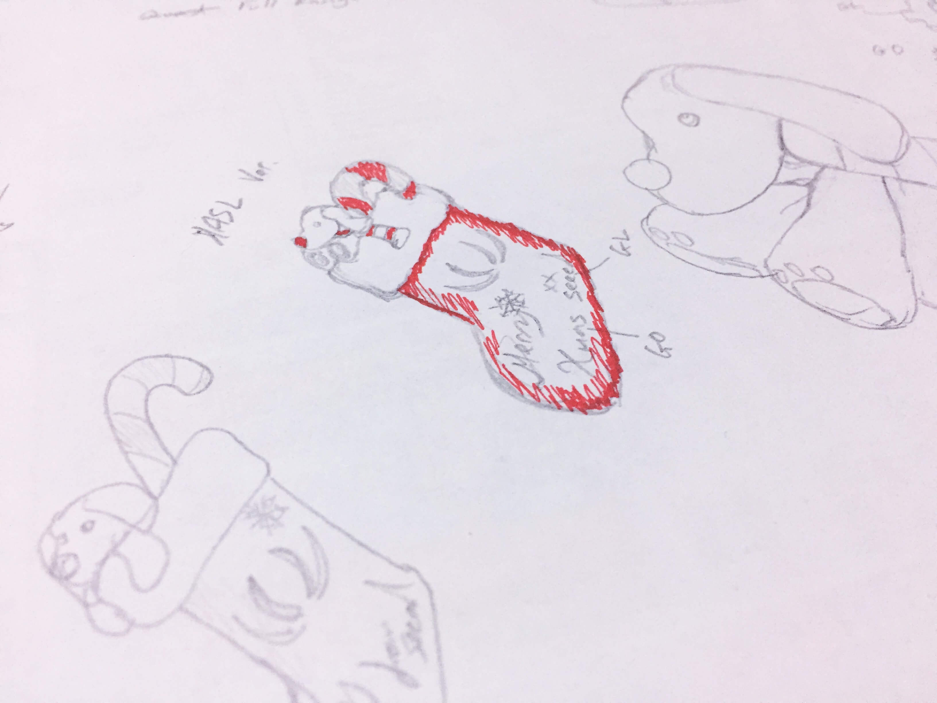
So, I wanted the design to be completely original, and I already had an idea of what I wanted to make. You could just find some images online and use those, but where is the fun in that? For the first attempt, it should be relatively simple while also presenting a challenge. Solder mask color and the subsequent range of colors that could be utilized was also an important consideration from the onset. After a few sketches, I came up with this:
Task 2: Import the design into Inkscape
The next step was to get it into Inkscape. Marc often held workshops guiding through the whole process. Unfortunately, I could not attend, but he told me that they would scan in the image and then trace it in Inkscape. But I was less confident in my hand-drawing skills than what I knew could be achieved in graphics packages, so I jumped straight into Inkscape to pen the design.
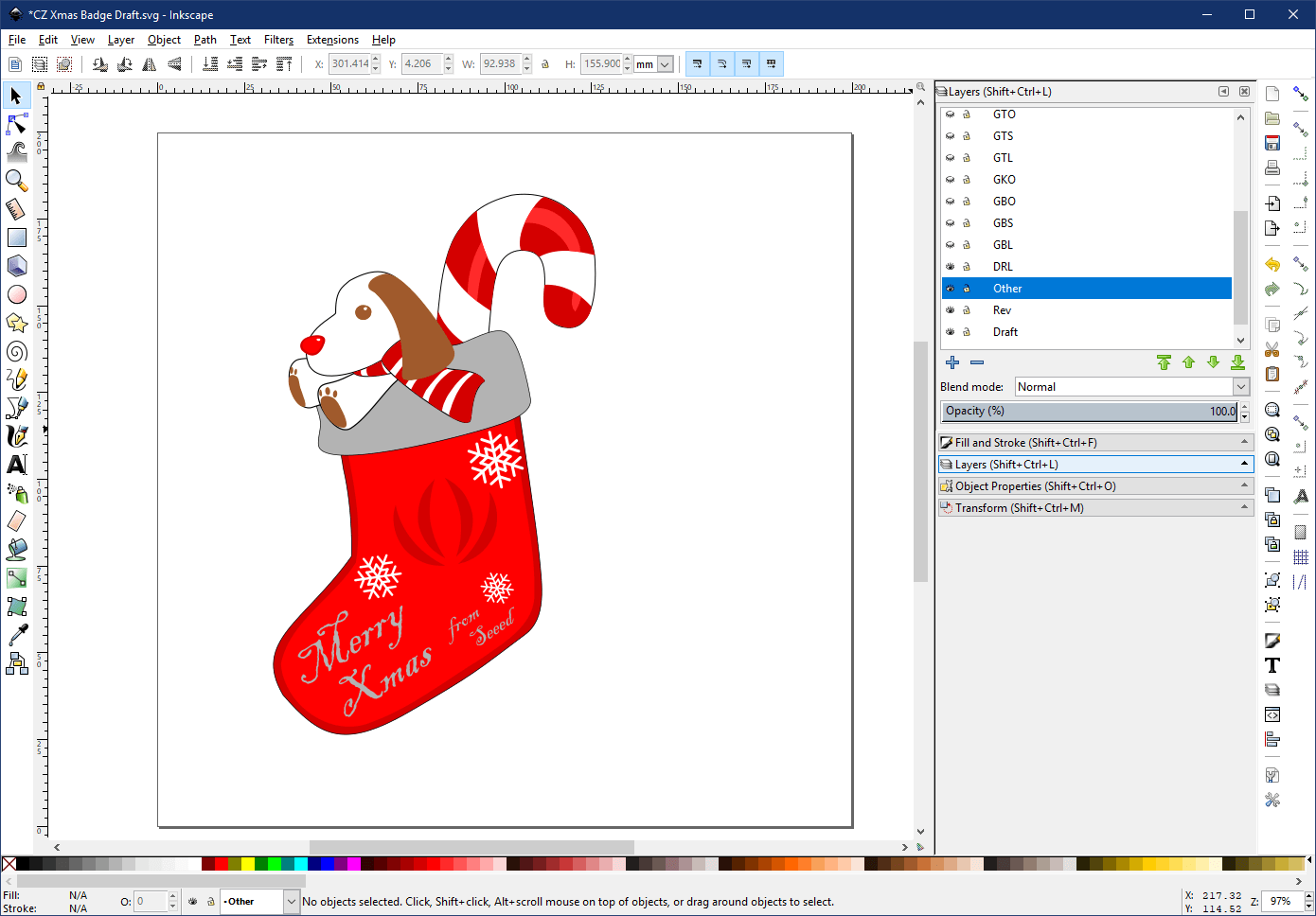
I had played around with the Microsoft vector graphics package a few years ago (I don’t remember the name), so I was familiar with paths and Bezier curves, and a few quick start guides later, the design was underway. It took a lot longer than I had anticipated though and ate up much of the weekend. Once I was happy with the overall design, it looked like this:
Task 3: Download and install the Inkscape extension
The extension itself is available on GitHub here, and the instructions are pretty simple. Extract it to your Inkscape extensions directory, and it will be available under the extensions tab in the toolbar.
Task 4: Prep the document
I think the extension was designed to be executed before beginning the design. This step prepares your Inkscape document into the respective Gerber layers and can set the document size. But it made more sense to me to get the final design done first in a “master layer” and then use that to work-out the Gerber layers, instead of jumping straight into Gerber. So if you make any mistakes, at least you can refer back to the master.
Task 5: Draw the Gerber layers
Now for the tricky bit: creating the Gerber layers. This is where my “expertise” comes in, but even though the basic rules are quite simple, executing it can be quite challenging. Especially, if you are not very familiar with Gerber files or are the type who exports Gerber files, doesn’t give them a second look then shoots them off to production. If you don’t know your GBO’s from your GTL’s then maybe you should look-up on the PCB manufacturing process and study some Gerber files.
Still confident? Good.
PCB Color Palette:
First off, a run through the basics. You typically only have one solder mask color to choose from, unless you have buckets for cash to pay for another solder mask coating, so making the most of the available colors is key to a great design. For the 6 solder mask colors available in Seeed Fusion, green, red, blue and yellow have the greatest range of what I will call “shades”:
| Name | Color | GTO (Silkscreen) | GTS (Solder mask) | GTL (Copper) |
| FR4 Substrate | Pale Yellow/Brown | N | N | N |
| Silkscreen | White (solder mask color may show through) | Y | N/A | N |
| Dark Solder mask | Dark shade and slightly translucent shade of the solder mask color | N | Y | N |
| Light Solder mask | Lighter/Warmer shade of the solder mask color | N | Y | Y |
| Surface Finish | Shiny silver for HASL, Gold for ENIG | N | N | Y |
The same idea applies to the bottom side.
For picky people, note that the precise shade of the solder mask oil and FR4 substrate may differ across manufacturers.
Black and white solder mask only have four different color options since the traces are barely visible under the solder mask. So they are not much fun.
Other notes to bear in mind before beginning;
– No silkscreen on copper: Generally, PCB manufacturers will remove any silkscreen on top of exposed copper/surface finish, so to be safe, don’t design anything on top of exposed copper.
– Bonus shades: Layers on the reverse side of the board can also affect the color on the front, especially for areas of bare substrate. For example, bare FR4 on the front side will look a little darker if the other side is covered in solder mask or copper. The effect can be very subtle though, and may only be obvious by holding the PCB up to the light.
– Don’t get too detailed: It can be tempting, and when you are working with PCB design, it can be easy to lose track of the sizes you are actually dealing with. But when CAM engineers process the files, they have an arsenal of programs to prep files for manufacture, for example: open up solder mask and silkscreen to copper clearances, copper to edge clearance, resize drill holes to match the available toolset etc. The smaller the features in your design, the more obvious these modifications become, especially for thin areas, so don’t overdo it. Your fab house won’t be pleased if you come back complaining about aesthetics.
– Bottom Layers: Don’t forget that the bottom layers are reversed! If you need text on the bottom layers, I recommend that you first reflect them, add any text, then reflect them back.
In this design, I tried to make use of all the colors options available to best effect. But despite knowing Gerber off the back of my hand, I made a few mistakes, and almost sent them to manufacture without realizing.
The most fiddly layer to get right is probably the solder mask layer since, in Gerber format, it is a negative rather than a positive like the other layers. So, the layer may not quite look like what you expect on the final board. I made that mistake and paid for it in delays.
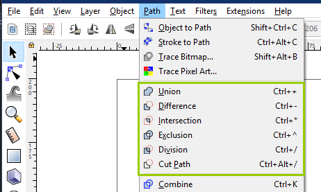
Another thing to know if you are not very familiar with Inkscape: These options under path will be indispensable for constructing the respective layers and will help ensure that positives and negatives match exactly in multiple layers. Get familiar with them, and perhaps learn the shortcuts.
Hopefully your design should look like something like this (top and bottom sides separated for illustration purposes only, they should be stacked and aligned together):

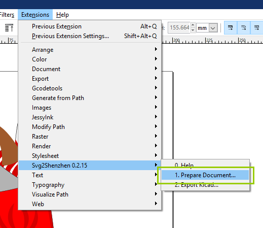
Step 6: Export the layers into KiCad
Time to work the magic with the SVG2Shenzhen extension. Bring up the Export KiCad window from the extension.
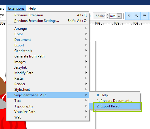
For entire PCB designs select “Export layers as… KICAD – PCB”. Everything else can be kept as the defaults. Let the extension work it’s magic and then check the resulting KiCad file.

During the design process, I figured that it would be better if I drew the artsy bits in Inkscape first, then used KiCad to draw the traces and footprints. That would save me from having to guess the sizes of the footprints and hand draw everything. But due to time constraints, the circuitry was left out. Oh well, next time perhaps.

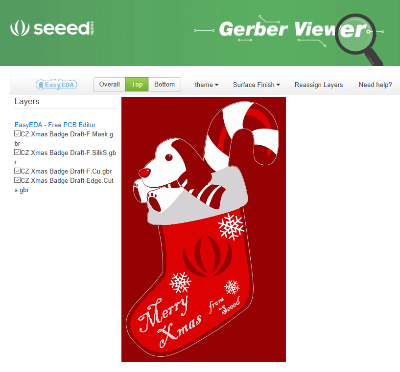
Step 7: Export the Gerber files from KiCad and send them to a manufacturer
Export the Gerber files as usual according to your chosen manufacturer’s guidelines. For the Seeed Fusion PCB manufacturing service, you can find our KiCad Gerber file export guide here. Then give the files a final check in a Gerber Viewer before shipping them off for manufacture!
Step 8: Wait for the boards to arrive and admire your creation!
I got lucky with my boards. I placed the order on Friday afternoon with the Seeed Fusion service and then picked them up on Monday afternoon. Just in time for Christmas Eve. In total, production was completed in less than 24 hours, without specifying any expedite service. Which helped with my 7-day challenge. I am not saying every order will be the same, I imagine the factory must have been less busy since it is the holiday period.
Here is how the stocking boards came out:


The verdict
Boards
I am quite happy with how the boards turned out. There are definitely some improvements for the next version but for a “first prototype”, if you like, they are pretty neat. I am particularly happy with how certain effects came out. All the snowflakes came out quite sharp and the alignment was very accurate. The photos do not do the HASL text’s shine any justice though, they have a lovely pristine shine to them and give the boards that needed Christmas sparkle.
However, in some pictures, you can see there is a red tinge to the silkscreen. I had not expected the solder mask color to come through so much. To remedy this for the next revision, I can just remove the solder mask oil from behind the silkscreen print. The light-effect on the candy cane didn’t quite have the effect I was expecting either. I was hoping it would give the candy cane a 3-dimensional effect, but the trace has its own 3D outline, which kind of draws away from the effect. Finally, I unintentionally left a red outline around the dog which further contributes to the red tinge.
Ease of Use
Actually, I spent a few days trying to work around some issues with the Inkscape extension. I had trouble getting all the layers to export correctly into KiCad and for each time, I needed to export the newest files to a new folder. For the export problem, it was because the colors I was using for the Inkscape layers were too “light”. Notice the threshold value in the Export KiCad window? If the threshold is too low or too high, it may not be able to distinguish from the color in your layers and the background. Simple solution, just use black and white.
In regards to my challenge, yes, I would have appreciated more time, but as always, the last minute rush up to Christmas is unavoidable. In total, the challenge went two days over, and I couldn’t design in any circuitry. A lot of time was spent fiddling with the extension itself and working out how to use it, and also drawing the Gerber files. It is not exactly easy to pick up but heck it was a lot of fun.
Now that I am more confident with the workflow and capabilities, things should go a lot smoother. I will definitely be using it again for the next revision, a fully functional badge version, and perhaps a Chinese New Year badge. The sky is the limit!
A huge thanks to the SVG2Shenzhen creator Budi Prakosa and contributors, and Marc for the inspiration! Check out the GitHub repository here.
Gerber files available on the Seeed Fusion Gallery, or order 10 pieces directly here.
Thanks for reading and Merry Christmas!
Thanks for the tutorial !
Anytime~