How to Export PCB Gerber Files from the Latest Eagle V9.4.2 the Easy Way
Is anyone keeping up with Autodesk Eagle updates? It seems like every week there is a new update but we are trying our best to keep up. This Gerber guide is for Eagle version 9.3.0 but has been updated for 9.4.2, which at the time of writing, is the latest version. Guides written for previous versions can be found on our FAQ page but please do exercise caution when following these since we can no longer guarantee compatibility. Now, without further ado, let’s begin!
For what seems like forever, Eagle has used a unique method for generating PCB manufacturing files. That is, all the settings can be packed into a CAM job file which users can apply directly. A manufacturer can configure this file and make it available to customers to ensure that the resulting files are compatible with their production guidelines.
It is a great and intuitive idea, particularly for beginners. No need to follow complex guides, match parameters or understand what weird settings mean. It’s a wonder why other software packages have not done the same.
With the latest versions, Eagle
In the following section, we’ll show you how to use them.
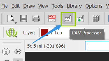
Open up your design and once your design is complete, and all the necessary checks have been made, find the CAM processor button on the main toolbar. Don’t click the one with the green arrow, this one will automatically use the default CAM file template which is not what we want.
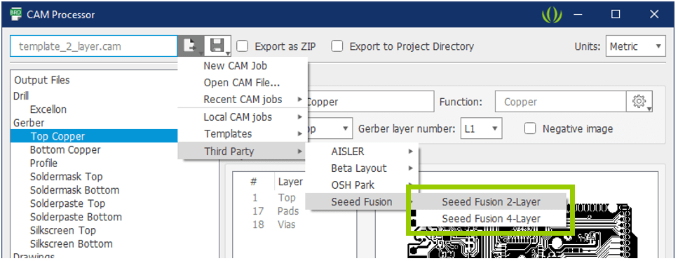
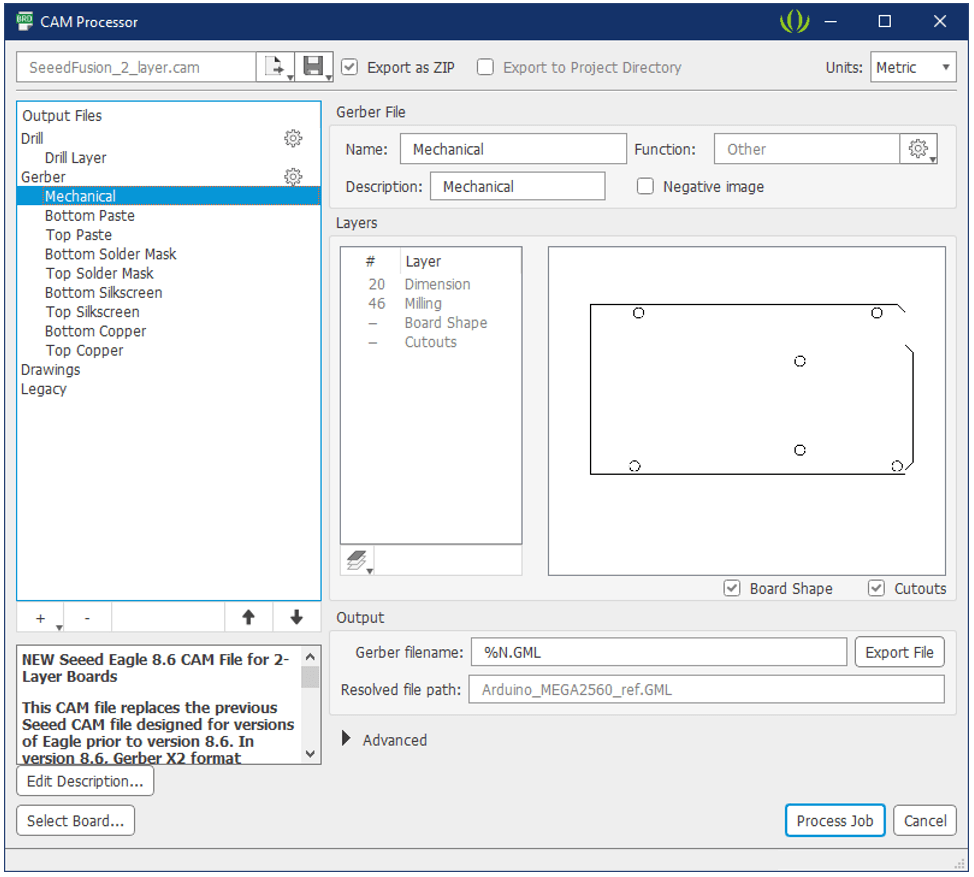
This will bring up the CAM Processor window, loaded with the template CAM file by default. We want to use the built-in Seeed CAM file to make sure it is compatible with the Seeed Fusion service. Load it up by clicking the file button on the top left and then go Third Party -> Seeed Fusion -> to find CAM files for double and four-layer boards. Select the appropriate one and your screen will look similar to the second window.
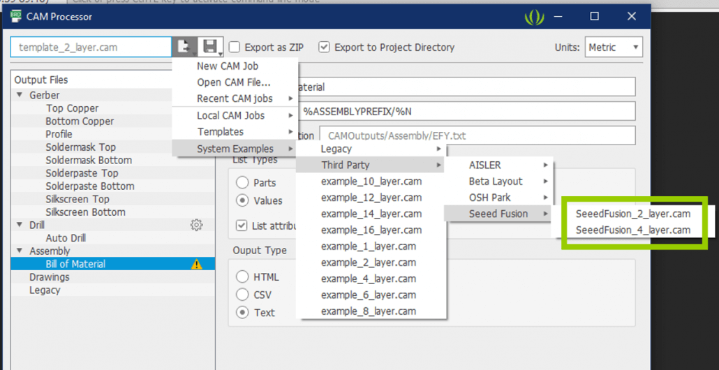
In the latest 9.4.2 update, the only difference is that the Third Party tab has been moved under System Examples (not sure why, makes grabbing a screenshot under a timed 5-second delay more challenging).
Ignore the description, this CAM file version remains compatible with later Eagle versions as well. We have tried to create the CAM file to be as “full-proof” as possible, so it should be compatible with many other PCB manufacturers. But as always, double check with your manufacturer first.
The later versions of Eagle have a built-in previewer like a Gerber viewer where you can view what exactly will be exported in each layer. We still recommend checking the files on another Gerber viewer though to be doubly sure that everything exported correctly.
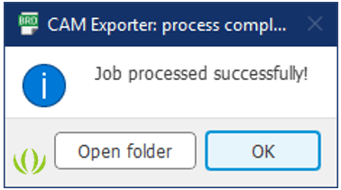
Then, once everything is ok, click Process Job and watch the magic happen!
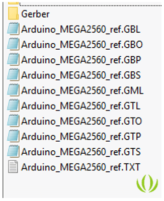
Eagle can export the individual files directly or export them as a pre-packed and gift-wrapped zip file. This zip file contains all the necessary manufacturing files and can be uploaded directly to most online interfaces like the Seeed Fusion PCB order page, or handed directly to your chosen manufacturer. Whichever method you choose, be sure to check that all the necessary files are present and contain data.
Why use the Seeed Fusion Eagle CAM Job files?
We have carefully chosen the settings based on our own experience with real customers’ Gerber files and general PCB practices. Every factory is different so it is your responsibility to verify that is compatible, but in the large majority of cases, these should be fine.
At Seeed, we take feedback very seriously and the following changes are based on the results of our investigations. For people who have a bit of experience with Eagle, here are the changes and the reasoning behind our decisions:
- Milling and Dimension layers: We’ve
included the milling and dimension layers (layers 46 and 20 respectively) in
the mechanical layer, so that all fabrication information on these layers like
labels for v-cuts are also passed onto the manufacturer’s CAM engineers. This includes
filled shapes that indicate cut-outs and slots which would otherwise be omitted.
While not the best option to indicate these features, we find that some
customers still have the tendency to use filled shapes and some older files may
not have been updated to the newest Eagle rules. This decision ensures compatibility
for most cases.
The argument against this is that things that are not necessary will also be exported in the mechanical layer but we say any weird stuff in this layer should be caught during DFM file review. Better to have too much information, rather than not enough and miss vital instructions that could render the board useless.
- Gerber Format: RS-274x Gerber format is selected to ensure compatibility with 99% of PCB fab houses. X2 is the new trend but there are still many manufacturers and older pieces of software that cannot read or have problems with this format.
- Negative Polarity: The negative image option is unchecked to prevent the issue of filled solder mask layers for RS-274x Gerber format (which could cause boards to come out naked!). This was an issue before that seems to be corrected in the latest Eagle versions but we can’t guarantee that it is not present in older versions.
- Use of Protel extensions for filenames: Protel PCB extensions were used to label layers in PCB manufacturing for decades, so much so that it pretty much became the standard for a number of fab houses, especially in China where Protel was and probably still is the most popular tool of choice. Standard naming is important for fab houses that may not speak English and can actually help automated software like Gerber viewers identify layers easily. Why it isn’t the standard, or being encouraged to be the standard is beyond us.
Sure, most CAM engineers are trained to recognize “solder mask” and “drill” and it is not difficult to guess which is which by the content, but every piece of design software uses different naming styles and it increases the likelihood of mistakes. Believe it or not, we still get files with ambiguous names, names in different languages or confusing labeling of top and bottom sides (A and B – guess which one is top and bottom? Answer is at the end of the article*).
Eagle is one of the most popular choices of software for customers of the Seeed Fusion PCB manufacturing service. While it has its flaws and caveats, it can satisfy 90% of our customers’ requirements. For more advanced features, you should communicate these directly with to your manufacturer beforehand.
The Seeed Fusion service specializes in hardware manufacturing services for PCB, PCBA, 3D printing and more. With over ten years of manufacturing experience, competitive pricing and an instant online quoting system, Seeed Fusion can provide mature manufacturing services for anyone, anytime. PCB prices start from just $4.90 for 10 pieces! Learn more.
We also love to keep a personal relationship with the community to understand their needs and troubles. Did you find this guide useful? We try to keep our documentation correct and up to date, but if you do find any problems or have some suggestions, please let us know.
In addition to PCB manufacture, Seeed also provides a full turnkey service, including parts procurement and assembly. Whether you are prototyping or scaling up to mass production, Seeed Fusion is the one-stop destination for smooth and hassle free PCB Assembly.
We offer various sponsorships and value-added services to provide an unrivaled PCBA experience aimed at minimizing setbacks and maximizing yield and efficiency while supporting developers. We include PCB DFM and PCBA DFA design checks, and functional testing for one piece free with every PCBA order, and offer free prototyping for business users and additional sponsorships for Raspberry Pi CM4, Raspberry Pi Pico, and Wio RP2040 designs.
Get an instant online quotation now, we look forward to working with you.
*A popular Japanese design program uses A and B to label the sides of a PCB board by default. For some reason, B is the top and A is the bottom. To make matters even more confusing, some customers also recognize this weird logic and will switch the names around! Japanese customers, you have been warned. Just use Protel extensions.