How to Generate PCB Gerber Files from Cadence Allegro/OrCAD – the Easy Way
Cadence Allegro and OrCad are the oddballs of the PCB EDA software giants. The software takes a bottom-up approach using various tools to make individual parts from pads to the final PCB layout. Those used to more beginner-friendly and self-explanatory programs such as KiCad and Eagle may be driven crazy by OrCad/Allegro’s counter-intuitive design flow and excessive right-clicking (me included). On the other hand, despite the steep learning curve, those weaned on the software find the level of customization and detail appealing, and develop a better overall understanding into what makes a printed circuit board and, more importantly, how this is communicated in the production files. It’s probably for this reason why OrCad/Allegro is still very popular and is often the software of choice for schools and businesses.
This comes at a price though, for both the user and PCB fab houses, particularly when it comes to exporting Gerber files for manufacture. The number of steps involved to just export a set of Gerber files leaves us craving a CAM file feature like in Autodesk Eagle. And we can’t help give off a little sigh every time we see the .art extension. But actually, the export method has a lot in common with Eagle and is difficult to get wrong with this method.
While the built-in documentation is comprehensive, simple, up-to-date and jargon-free guides for OrCad/Allegro are rather scarce. Methods for exporting Gerber files from OrCad/Allegro vary and are sometimes incomplete or not fit for the purpose of sending off the data to be manufactured for example with the Seeed Fusion service.
We once had an entire class of students fumble with problems with board outlines and just getting the bare minimum data to us was a pain. Even the professor was struggling.
Seeed Fusion Customer Service Operative
So, if you are struggling to export PCB Gerber files from OrCad or Cadence Allegro successfully, we hope this guide will help you with your woes once and for all.
To begin with, what we and most PCB fab houses typically need is contained in the list below:
|
Gerber/Drill |
OrCAD/Allegro |
Standard File Extension |
| Top Silkscreen (optional) | GE – Silkscreen_Top | .GTO |
| CO – Silkscreen_Top | ||
| Top Solder Mask | SU – Soldermask_Top | .GTS |
| Top Copper | SU – Top | .GTL |
| Outline/Mechanical | GE – Design_Outline | .GKO/GML |
| GE – Cutout | ||
| Bottom Silkscreen (optional) | GE – Silkscreen_Bottom | .GBO |
| CO – Silkscreen_Bottom | ||
| Bottom Solder Mask | SU – Soldermask_Bottom | .GBS |
| Bottom Copper | SU – Bottom | .GBL |
| Drill File | NC Drill | .DRL or .TXT |
| Top Paste (for stencils) | SU – Pastemask_Top | .GTP |
| Bottom Paste (for stencils) | SU – Pastemask_Bottom | .GBP |
Apart from the silkscreen layers, all the other layers are pretty much essential for a typical two-layer board. For multilayer boards, make sure you export all the copper layers as necessary. If you need the paste layers to make PCB stencils, you can export them in a similar way.
In OrCad/Allegro, these Gerber ‘layers’ are referred to as ‘films’, a reference to how photo imageable films are used to print the pattern onto the board.
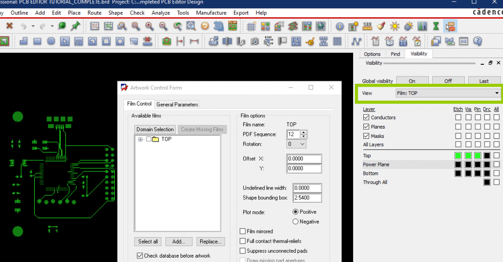
Before we export these, we’ll make some data-sets containing the essential features. These are based on Views that you may already be familiar with while making the layout since they are useful in switching between the many layers.
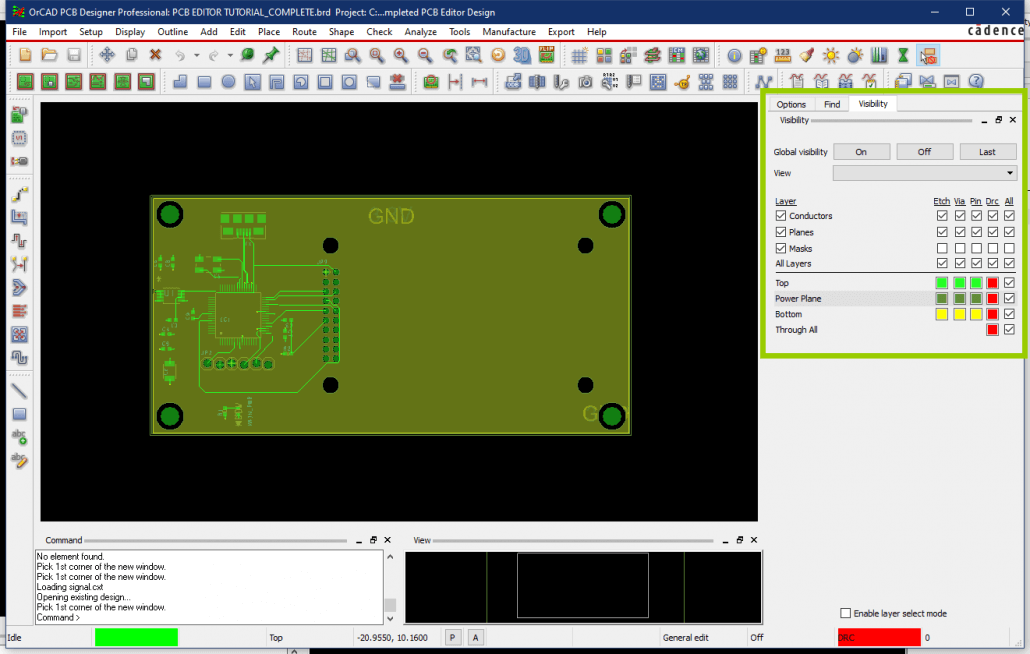
By default, the Visibility panel is on the right of the screen when modifying a .brd file. Here you can select different subclasses of the PCB to display on the main window. What we want to do is group sets of features for each of the respective Gerber layers in a View. At first, the Views drop-down box may be empty. But we can add some by doing the following:
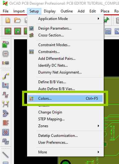
Go to Setup on the main toolbar and Colors… to open up the Color Dialog or press Ctrl+F5 for the shortcut. Don’t be put off by the sheer number of options and boxes. OrCad/Allegro has a wealth of features for many advanced and specialized designs that we’ll probably never use. As one becomes more familiar with PCB design, these other features may come in handy.
Stack-up is the class that appears when the dialog is opened up. Here the information, or objects, for the copper, solder mask and paste layers are available. Repeat the below instructions for each layer to group the necessary objects and save them into a View.
1. Open the Color Dialog window by going Setup -> Colors…
2. Turn off all layers by setting Global Visibility: Off on the top right.

Then, click the leftmost All checkbox by the corresponding sub-class for the layer you are making (e.g. Paste Top). This selects all the boxes to the right and these objects will appear on the main window. Click ok to exit.

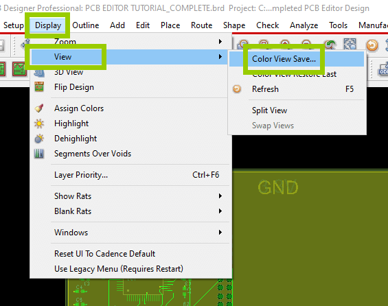
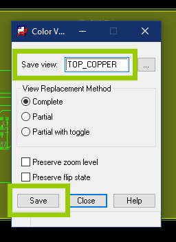
Save this view by going to Display on the main toolbar -> View -> Color View Save… Then give the layer a name (you can refer to the table before), click save and close the window.
Repeat this for the other layers, both top and bottom for a two-layer board, remembering to uncheck all other layers each time.
Copper Layers (repeat for bottom):
– Stack-Up -> Soldermask_Top
Solder mask Layers (repeat for bottom):
– Stack-Up -> Soldermask_Top
Paste Layers (repeat for bottom):
– Stack-Up -> Pastemask_Top
For the silkscreen layers, they consist of two parts: the component outline and the designator or reference. The former is located under Stack-Up class like before but the designators are located under Components.
Silkscreen (repeat for bottom):
– Geometry -> Silkscreen_Top – For component outlines
– Components -> Silkscreen_Top – For component designators
For the board outline, we personally prefer that all the mechanical elements such as cutouts, v-cuts and the board outline be included in the outline Gerber layer. This avoids confusion and is clearer for the engineers reviewing the files. To do this make a view that includes the following:
Outline Layer:
– Geometry -> Design_Outline
– Geometry -> Cutout
And if there are features drawn in other sub-classes they should also be included. Some manufacturers ask that the board outline be included in the other layers as well. If that is the case then you can just select these subclasses as well when creating the other layers.
Now that we have our views saved, they will appear in the Views drop-down list. These are useful in reviewing your design in terms of manufacturing data. We will use these to create the films and export the Gerber files for the fabricator.
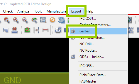
On the main toolbar, go to Export -> Gerber… and the Artwork Control Form window will appear.
With this window open, select the view for the layer you want to create the Gerber file for in the main window.
Then in the Artwork Control Form window, right-click a folder already present in the Film Control tab under Domain Selection and select Add.

Enter a name for the Gerber file and select ok. Spaces are not allowed.
Change the Undefined Line Width to 0.1mm.
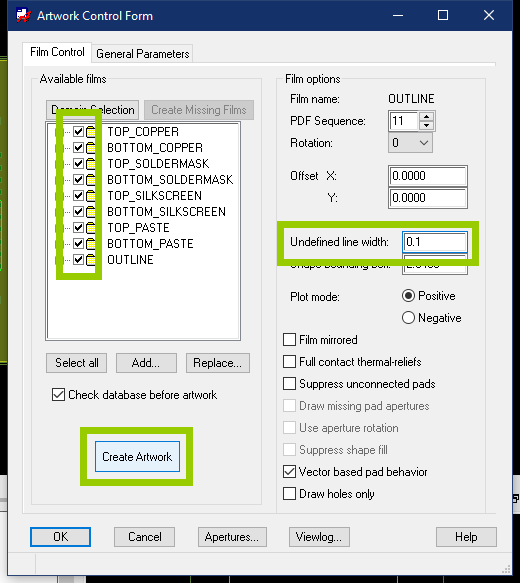
Repeat steps 2-5 for all the Gerber files and once done, select all the layers you just created and click the Create Artwork button. The software will generate your Gerber files in the same directory as your design file and in a folder called artwork, and display a log file. But we’re not done yet. We still need to generate the NC Drill file in Excellon format to indicate where all the drill holes on the PCB need to be and of what size.
To do this go to Export -> NC Drill and a new window will appear.

By default, OrCad/Allegro does not export the drill file in Excellon format so we need to check the Auto tool select option and go to NC Parameters. Check the Enhanced Excellon format option in the new window and close it.
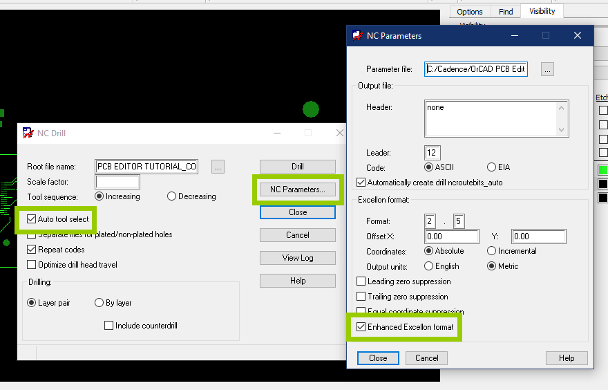
Back in the NC Drill window, click Drilland the drill file will be generated and placed in the same directory as the Gerber files.
All done! Package the Gerber and drill files together (without all the other stuff) into a .rar or .zip file and give them a final check in a separate Gerber viewer software. Once everything is verified, hand them over to your preferred manufacturer and wait for your PCBs to arrive.
Common Problems:
Missing solder mask and drill layers: Often we just receive just Top, Bottom and Outline files but at the bare minimum, we also need the solder mask and drill hole files. The absence of either of these files could be misinterpreted as meaning they are not needed, which could be disastrous. We have a hunch that this problem is encouraged by some documentation that splits the generation of these files into separate steps, which causes the other layers to easily be missed. Don’t fall for this trap.
No Board Outline: Happens a lot, not just with OrCad/Allegro. Make sure the outline is drawn in the Board Outline subclass and this is selected in the view.
No Drill File: Unlike the artwork files, the drill file is exported in the project directory and by default is named after the project file so it can easily be missed. Find the file with the .drl extension and make sure it is included in the package.
Incorrect file extensions: Not actually a problem since the extension is just a label to tell us which file is which. It has nothing to do with the format of the files but many manufacturers request that standard extensions are used. OrCad/Allegro does not have the option to add a unique extension for each file but so long as the names clearly indicate the respective layers then you should be fine. If you really want, you can just change the extensions directly by renaming the files.
Too many files: OrCad/Allegro exports all files in the same directory as the .brd file, including a lot of log files. Just trying to find all the manufacturing files can be a pain so please don’t send all of this to the fabricator. No one wants to waste time going through each file trying to guess what information is important.
At Seeed Fusion, you just need to upload this package onto the website and fill in some parameters to get your PCBs manufactured. With the instant and live online quoting platform, there is no need to wait around for prices. Seeed has over ten years of experience in manufacturing and supply chain management in the heart of China, so your boards are in safe and professional hands. Get a competitive quote online now starting from just $4.90 for ten pieces. And if you need assembly as well, Seeed provides a complete turnkey service with full online BOM quoting, components procurement and in-house assembly for prototyping to mass production needs.
Try with our 5 pieces free assembly offer – just pay for components and the PCB. No assembly fees, operation fees or materials fees and shipping is free for all PCBA orders.
I have been using Allegro 17.2 daily for the last 2 years, and it still makes me want to rip my hair out at how complicated Cadence makes things. I started out with Eagle, went to Altium (still my favorite, by far), use Circuit Maker (Altium lite), and currently Cadence.
You’re tutorial is right, but could be simplified a little, by just using the Artwork Control Form and just setting up the layers you want (unless you don’t know which layers you need, but that’s another story).
In my limited experience, Cadence is NOT worth the money they charge for their software. It’s bloatware, it crashes, the program doesn’t operate like any/every other piece of Windows software, and things are hidden everywhere, or the same operation can be completed 5 diff ways, just cluttering things up.
Just my $0.02.
Can’t help feel slightly sorry for you. We don’t have a lot of experience using it but I was surprised how difficult it was just to even install and find out how to open the PCB editor. Despite that, we often encounter beginners using Cadence to design their first PCB.