Seeed Studio’s Main Quickturn PCB Factory Upgrades the Silkscreen Line
To pass IPC Class 2 quality control standards, the only requirement for silkscreen printed text on PCBs was that the text is ‘readable’. But every now and then, we used to receive messages from unhappy customers complaining of poorly printed silkscreen – maybe sections were faded or the entire silkscreen layer was misaligned with the rest of the board, etc. While purely aesthetic, we know that our customers have high standards when it comes to the appearances of their boards. So, we are very pleased to announce that back in September, Seeed Fusion‘s main quickturn PCB factory upgraded its entire silkscreen printing line to use automated ink-jet printers.
What does that mean exactly? In a nutshell, its bye-bye misalignment and fading issues, as well as a reduction of the time for silkscreen application.
How is silkscreen applied traditionally?

Traditional silkscreen printing is exactly that, large silk webbing with photoresist is stretched in a frame and a liquid mixture is squeegeed through onto the PCB surface. The silks are prepared the same way in which solder mask and copper layer silks are made.
A negative of the silkscreen Gerber layer is printed on a sheet of dry film, liquid photoresist is applied, dried, UV activated and then the exposed areas are rinsed off. The non-activated areas will block the ink during the actual silkscreen printing process.
Then the framed silkscreen is locked into a workstation, and the silkscreen ink is squeegeed over the surface of the PCB under the silk. The PCBs are then cured in an oven for 10-15 minutes.
While the application process is very quick, much time and energy is spent in preparing the actual silks. By using inkjet printers, we can cut this time and save on materials, but most of all, drastically improve the consistency of the printing.
How is the silkscreen applied with an inkjet printer?
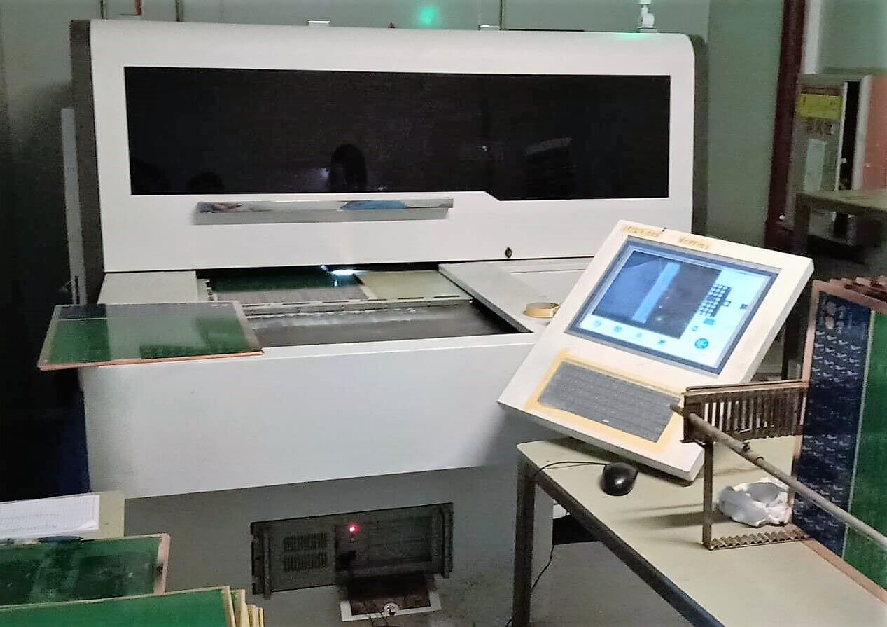
A new inkjet silkscreen printer
Using a designated PCB inkjet silkscreen printer, like the one shown below the PCB panel is placed inside the compartment and the machine does the rest.
The panel is locked in place and moved into position. Then an internal camera then uses the panel fiducial marks to correctly align the panel which prevents alignment issues. A preview of the boards can even be viewed on the monitor before application.
The printer then precisely sprays micro-droplets of ink onto the surface much like a typical household printer. The boards are then cured in an oven for ten minutes.
How do the two methods compare?
Clearly, the inkjet printing method is a lot simpler and requires a lot less labor. The dry film process is eliminated completely and so there is no need to make, store, then dispose of the huge framed silks.
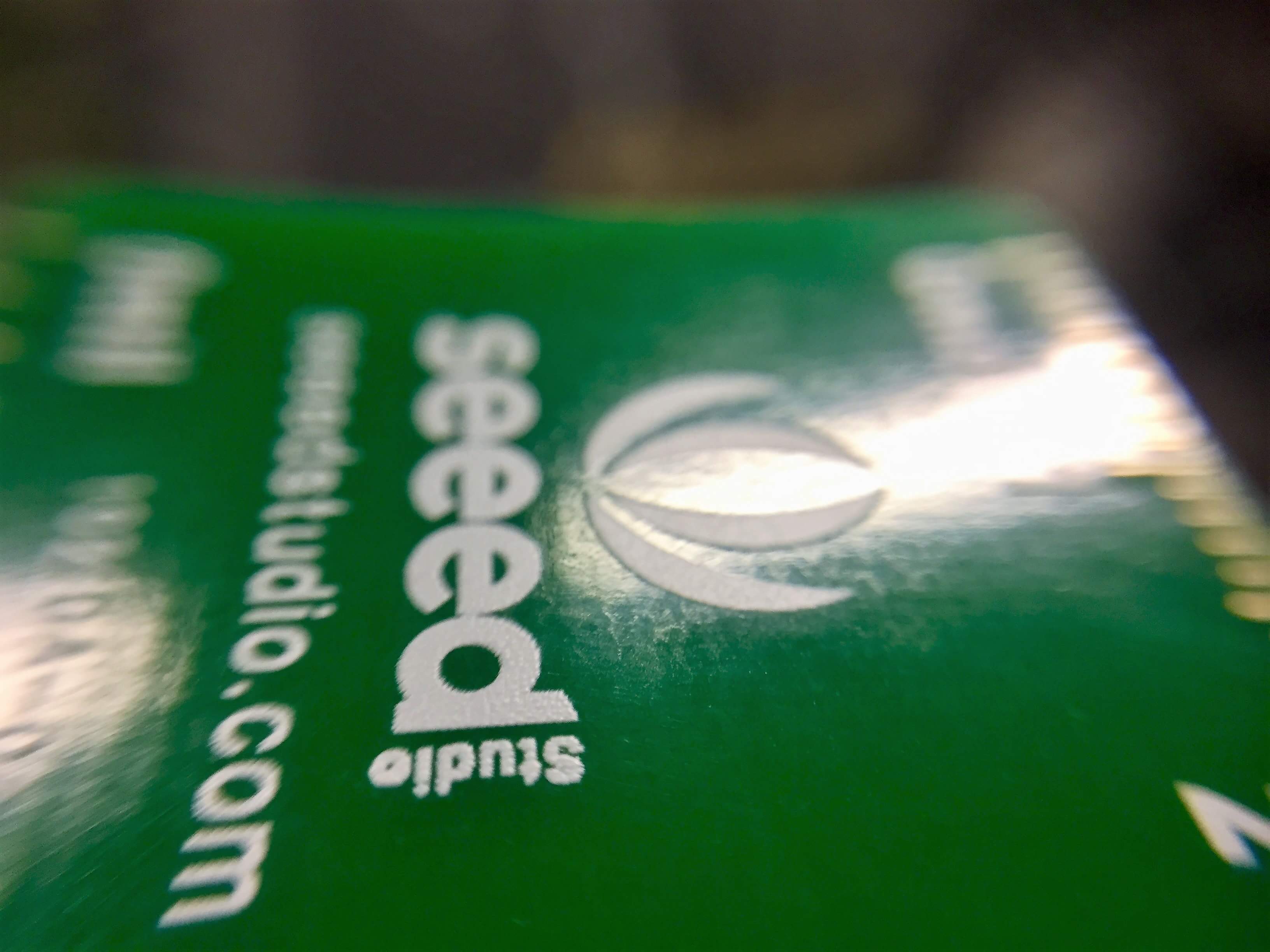
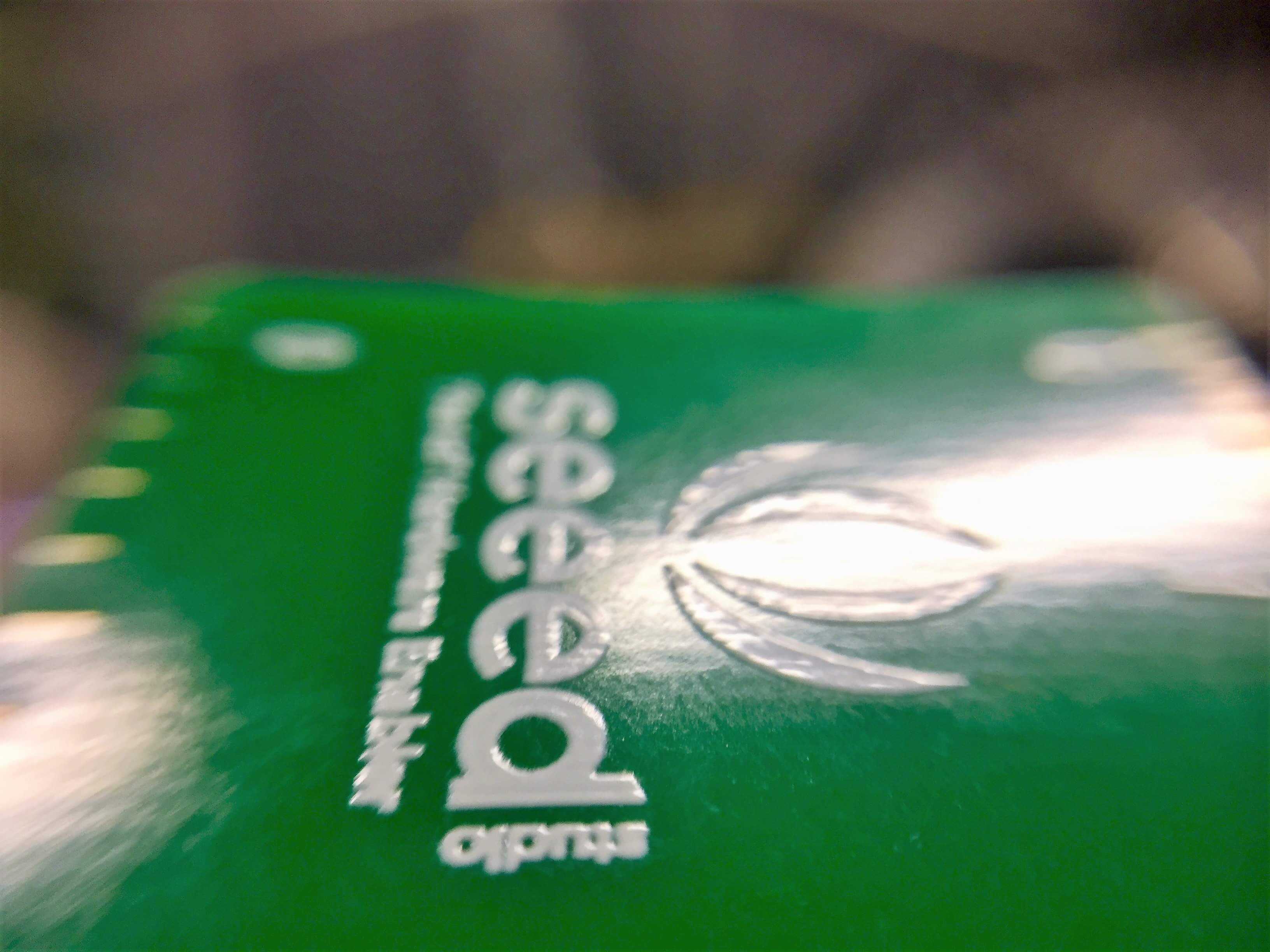
But besides consistent printing, guaranteed alignment, and no fading, how does the printing quality of the inkjet compare? Conveniently, we have a sample of our Seeed Fusion rulers printed using manual silkscreening and one printed using the inkjet and we thought we’d share our verdict with you.
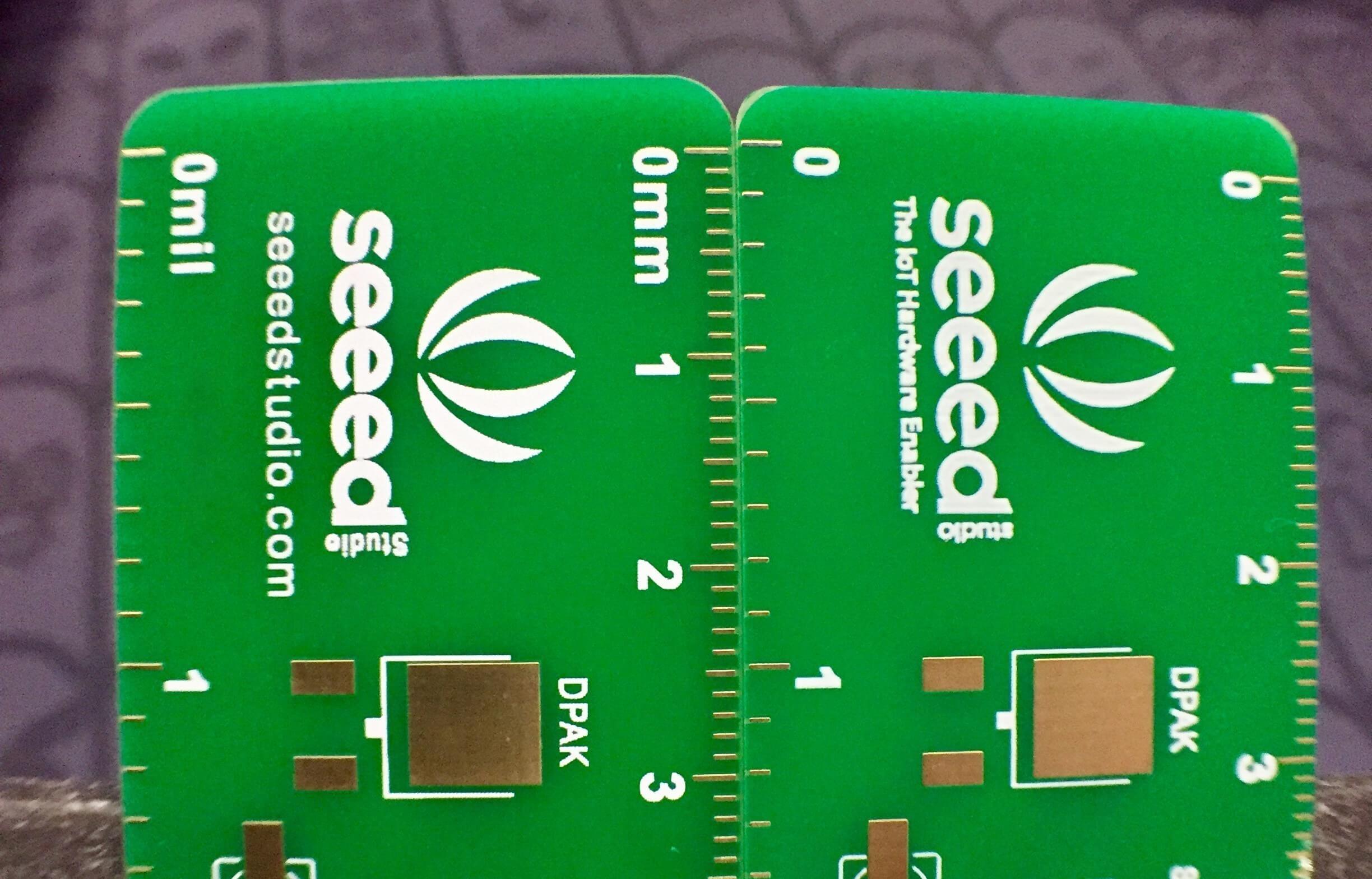
Manual silkscreen on the left and inkjet silkscreen printing on the right
Sharpness: This is a classic sharp but grainy versus smooth but fuzzy argument. As you can see from the pictures, the inkjet on the right is not as sharp as the one on the left but it does have a nice smoothness to the edges. Right up close, the graininess of the silk sample starts to become really apparent. You can almost see the “pixels” of the silk holes.
From far away however, it is barely noticeable and the only thing that stands out is that the silks do look a bit sharper but the inkjet has a nice embossed glossy feel to them that gives them a sense of quality. We didn’t do a scratch test, but we just feel like the inkjet would last more wear and tear compared to the silks which have a flat and kind of chalky appearance.
Precision: In this comparison, the alignment in both are pretty good. It is only really noticeable on one of the IC footprints. The logo is not a good comparison since the surrounding text in the new logo is a lot smaller in the inkjet version. While fading is not a problem in this case, there is still some evidence of fading on the bottom footprint.
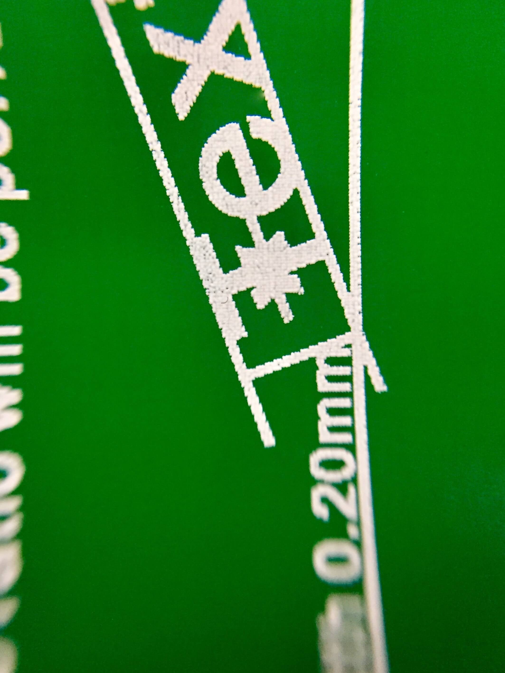
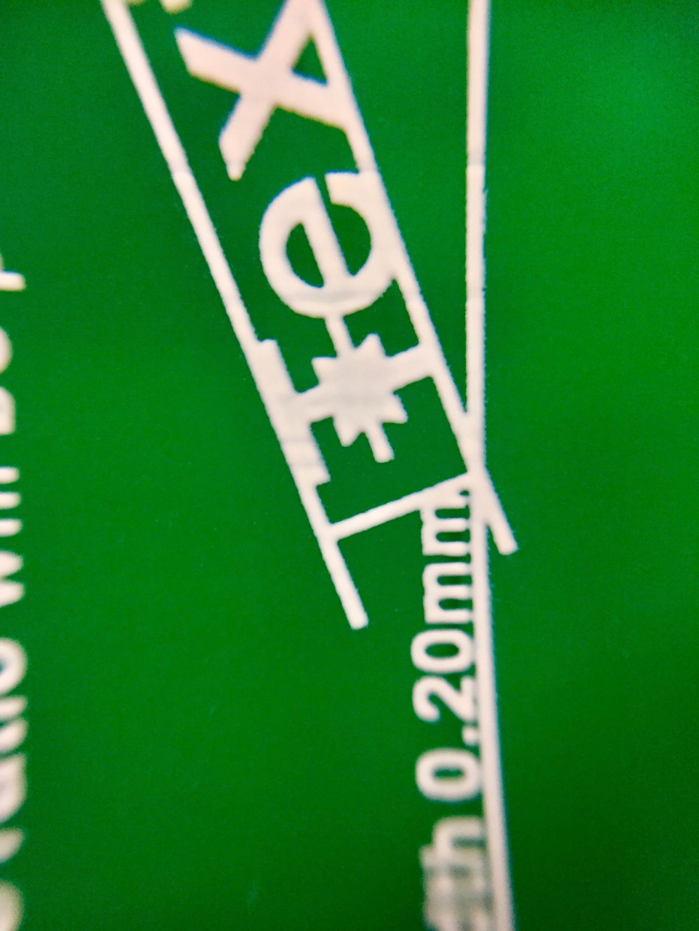
 Notice how the silkscreen component outline is shifted upwards for the TSSOP28 footprint and the QFP32 outline has faded
All in all, we hope you won’t be so picky as to compare such fine details. We hope you will appreciate the advantages of consistent and uniform printing, faster operations and increased efficiency as a result of the upgrades. See for yourself with the Seeed Fusion Quickturn PCB Service.
Have you noticed the change? What do you think?
You may also like:
SEEED FUSION SERVICE INCREASES DISPATCH EFFICIENCY WITH WAREHOUSE OPERATIONS UPGRADE
WHY PRODUCTION LINES NEED TO BE CAREFUL WITH WS2812B RGB LED ASSEMBLY
NEW SEEED FUSION PREMIUM PCB SERVICE FOR INDUSTRIAL APPLICATIONS AVAILABLE NOW
Hi,
How to get such a ruler 🙂 ?
Alex
Hi Alex,
You can get buy some here
https://www.seeedstudio.com/Seeed-Studio-PCB-ruler-X-5-p-2990.html
Or download the Gerber files here, we’ll update the Seeed Fusion Gallery with the newest files soon.
https://www.seeedstudio.com/Seeed-Studio-Fusion-PCB-Ruler-445-g-1048700?source=distributors&ac=1a63e00be005b92b55febbf5e99a5675&source=distributors&ac=1a63e00be005b92b55febbf5e99a5675
Enjoy!