13 Common PCB Soldering Problems to Avoid
Hand soldering has always been considered a hallmark skill to have in every electronics maker’s repertoire of geeky skills. Soldering has never been rocket science. It can be a fun activity for beginners to try out and with enough practice, it is an easy skill to pick up.
Although it is possible for anyone to throw down solder onto PCBs, whether you get classy solder joints or downright caveman quality ones is a different matter altogether. With components becoming smaller and more compact, the chances of soldering issues occurring have become higher. When soldering the PCB, try to make the finished product have the following characteristics:
- The soldering surface is kept clean;
- The solder joints must have sufficient mechanical strength to prevent the soldered parts from falling off or loose under vibration or impact;
- The soldering must be reliable and ensure electrical conductivity This is not only a guarantee for the product’s function but also to prevent the product from being burned out by a short circuit.
And if your PCB is going to be used for an important application, it will be more important than ever to know what a good solder joint looks like.

(Source: Surfacemountprocess)
Here’s a guide to help you discern what’s good and what’s not, so that you may be sure to avoid these soldering issues for your home projects, or just to be able to do a quality assessment on assembled PCBs received from a third party.
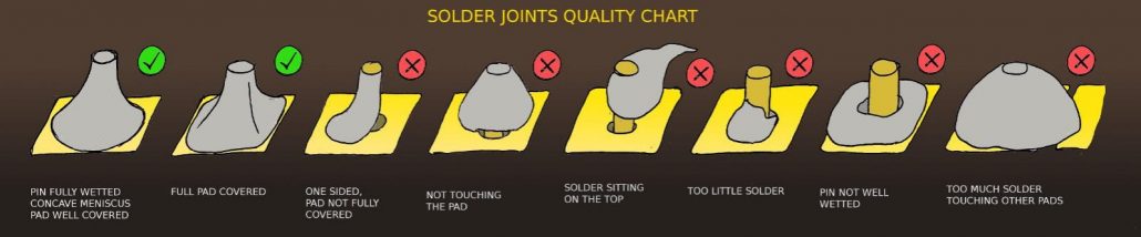
Ideal Solder Joints
When looking for solder defects, it’s helpful to have an image of an ideal solder joint for comparison.
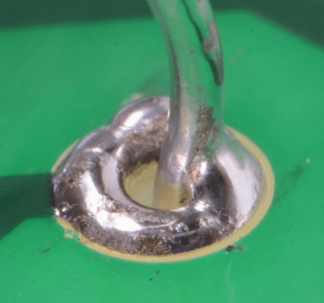
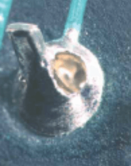
The Ideal Through-hole Solder Joint – It’s like a Hershey’s Kiss
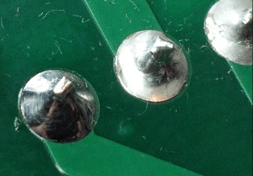
An ideal through-hole solder joint
(Source: unbrokenstring)
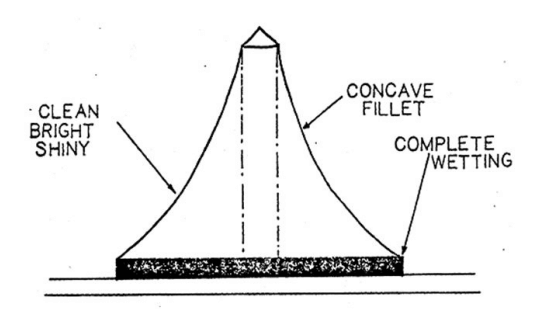
The ideal solder joint for through-hole components is a “concave fillet”, which has a smooth and shiny concave surface at an angle of 40 to 70 degrees from the horizontal, which looks just like the shape of a Hershey’s kiss. It can be achieved when the soldering iron is at the right temperature, with the oxide layer cleaned from the PCB contacts.
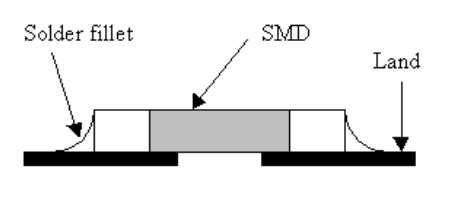
The Ideal Surface Mount Solder Joint
Similarly, good SMD solder joints have smooth, concave fillets as well.
(Source: poeth)
Hence, the general characteristics of a good solder joint:
– Has good and complete wetting
– Has a concave fillet
– Is shiny and clean
Bad Solder Joints
Unfortunately, there are many ways for solder joints to go wrong, as solder always seems to go where it isn’t supposed to.
(Source: gaudi.ch)
1. Solder Bridging
Nasty solder bridges – through-hole and surface mount
(Source: Pimoroni, Youtube-Androkavo)
Of the many problems caused by smaller and smaller components, solder bridging takes the top of the list. A solder bridge is formed when two points on the circuit board that should not be electrically connected are inadvertently connected by solder during PCB soldering. This will form an electrical short circuit, which may cause various damages, depending on the circuit structure.
It usually due to the excessive application of solder between joints or using soldering tips that are too big or too wide. Or the angle when the soldering iron is withdrawn is inappropriate. Identifying a solder bridge can sometimes be challenging, as solder bridges can be microscopic in size. If left undetected, it can lead to a short circuit and cause a component to burn up.
A solder bridge can be fixed by holding your solder iron in the middle of the bridge to melt the solder, and drawing it through to break the bridge. If the solder bridge is too large, excess solder can be removed a solder sucker.
Of course, it is best to prevent the formation of solder bridges; you can use the correct lead length for the through-holes. The lead length suitable for your application depends on the size and thickness of the PCB and the size and quality of the components; in addition, you should use the correct hole size and Land diameter for through-hole parts.
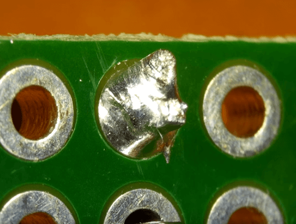
2. Excessive Solder
(Source: Androkavo, Youtube)
If you get too enthusiastic and apply too much solder onto a pin, excess buildup is what you’ll get, characterized by its rounded and raised shape. The direct reason is that the solder withdrawal is too late.
A common beginner’s assumption is the more solder the better but while more solder should increase the amount of material forming the joint, it is difficult to know what actually happened beneath that mass of solder. There still lies a possibility that neither the pin nor the pad is properly wetted. On the one hand, this wastes solder, on the other hand, it increases the risk of solder bridge formation and may contain other defects; So it’s better to be safe than sorry. Enough solder to adequately wet the pin and the pads thoroughly is usually sufficient and the concave surface remains the best shape to have as it allows us to better access the wetting of the joint.
Therefore, the key to avoiding too much solder is to grasp the timing of solder withdrawal.
3. Solder Balling
Solder balls are also one of the most common soldering defects that occur typically with wave or reflow soldering. It appears as a small sphere of solder that adheres itself to a laminate, resist, or conductor surface.
Solder balls may be caused by many factors, mainly due to the following two reasons:
- When soldering printed boards, the moisture near the through holes on the printed board will become steam due to heat. If the metal plating of the hole wall is thin or there are gaps, the water vapor will be removed through the hole wall. If there is solder in the hole, the water vapor may extrude the solder and produce solder balls on the front side of the printed board.
- The solder ball produced on the reverse side of the printed board (the side contacting the wave crest) is caused by improper setting of some process parameters in wave soldering. If the amount of flux coating is increased or the preheating temperature is set too low, it may affect the evaporation of the components in the flux. When the printed board enters the wave crest, the excess flux will be evaporated at high temperature and the solder will splash out from the tin bath. Irregular solder balls are produced on the printed board surface.
4. Cold Joint
(Source: Androkavo, Youtube)
The surface of cold joints appears dull, lumpy, and pock-marked. This is typically caused by insufficient heat being transferred to the joint to completely melt it which may be a result of a number of different things. The soldering iron or the joint itself may not have been given enough time to heat up sufficiently, the iron temperature may not be set high enough to melt the particular solder type being used (e.g. lead-free solder has a higher melting temperature) or, it may be a result of the design of the pads and traces themselves. For example, a pad connected directly to the ground plane without thermal relief considerations will cause the heat of the soldering iron to be lost to the ground plane. If you find a stubborn solder joint that refuses to liquify then the design may be at fault.
Cold Joint is the same as virtual welding. It is difficult to fully expose during the production process. It often requires users to use it for a period of time, which may be days, months, or even years. This will not only have extremely bad effects but cause extremely serious consequences. Because the strength of cold welding is low, the conductivity is not good.
5. Overheated Joint
Just as too little heat will cause wonky joints, too much heat will also give you a splitting headache. Overheated solder joints have white solder joints, no metallic luster, and rough surface. Overheated solder joints can result from the soldering iron temperature being set too high, or result from solder failing to flow, possibly due to the surface of the pad or lead already having a layer of oxide, preventing sufficient heat transfer and therefore leaving you heating the joint for too long. Hopefully, the damage caused will not be severe (perhaps just some burnt flux) but it may cause pads to lift entirely, killing the board or requiring costly repairs. Avoid this by choosing the correct solder iron temperature and use flux to clean dirty looking joints and pads.
6. Tombstoning
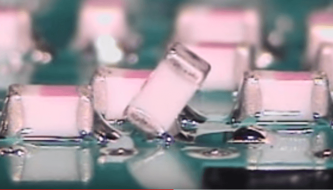
The tombstone defect – surface mount and through-hole
(Source: Youtube – BermNarongGamer, Epectec)
A tombstoned component is usually a surface mount component, like a resistor or a capacitor, with one side lifted off from the pad. Ideally, the solder will attach to both pads and begin the wetting process. But if the solder on one pad has not completed its wetting process, one side of the component will tilt on its side, looking like a tombstone, and hence its ominous name.
For reflow soldering, anything that would cause the solder paste on one pad to melt before the other can cause tombstoning. For example, lack of thermal relief design or unequal thicknesses of the traces that connect to the pads. For wave soldering, components with large bodies may be physically pushed by the incoming solder wave, causing the component to be fixed in the tombstone fashion. Layout engineers must consider the direction of the wave when designing boards destined for wave soldering.
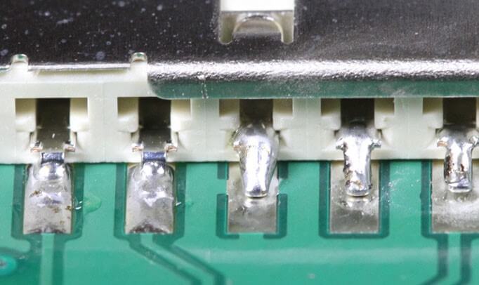
7. Insufficient Wetting (Through-hole)
Joints that are not fully wetted are weak and do not form a strong connection with the board. Ideally, the solder should achieve 100% wetting with the pad and pin, leaving no gaps or spaces exposed. Insufficient wetting of the pins and pad results from failure to apply heat to both the pin and pad, and not giving the solder enough time to flow. Most of the reasons are that the surface of the welding area is contaminated, or is stained with solder resist, or a metal oxide layer is formed on the surface of the bonded object. The technique to repair this is to clean the board thoroughly and evenly heat both the pad and the pin.
Products with Insufficient Wetting problems have low strength, and the circuit is not connected or on and off.
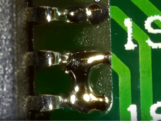
8. Insufficient Wetting (Surface Mount)
Similarly, SMD components can also suffer from insufficient wetting. In the image above, 3 pins of an SMD component do not have good wetting with their respective pads. The solder on the pins had failed to flow onto the pads, as the pin was heated instead of the pad. This will cause missed soldering or less soldering failure, which may cause components to fall off.
The solution to repairing this defect is to heat the solder pad with the tip of your soldering iron, then applying more solder until it flows and melts together with the solder already on the pin.
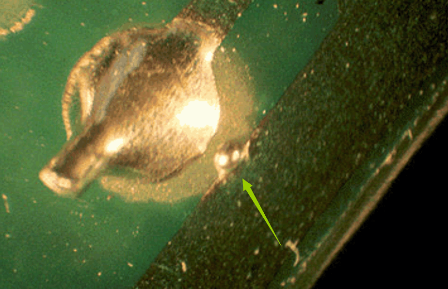
9. Solder Skips
(Source: Epectec)
A solder joint that is not wetted with solder is generally referred to as a solder skip. There is a clear dividing line between the solder and the lead of the component or with the copper foil, and the solder is recessed toward the dividing line. It occurs when solder skips over a surface mount pad, resulting in an open circuit. The solder surface in contact with a component is like a balloon pressing against the walls of a room – in a tight corner, due to the high surface tension of the molten solder. The cause of solder skips can be a combination of slip-ups in the design or during manufacturing.
You may have placed down an uneven pad size, or your manufacturer could have used an incorrect wave height between your board and the soldering wave.
The harm is that it may cause the circuit to not work properly.
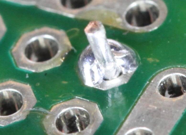
10. Lifted pads
A lifted pad is a solder pad that has become detached from the surface of the PCB possibly due to excessive force on an existing joint or excess heat. Another possibility is that the position of the pad is below the component, which is in the blind spot of the repair technician. Therefore, the technician may try to move the component because the solder joint cannot be seen during the operation, causing the pad to tilt.
Such pads are difficult to work with since the pad is very fragile and can easily tear from the trace. In fact, these printed boards have been damaged.
If you still want to use this PCB,you can try the remedy. Every effort should be made to adhere the pad back onto the board before attempting to solder to it.
.
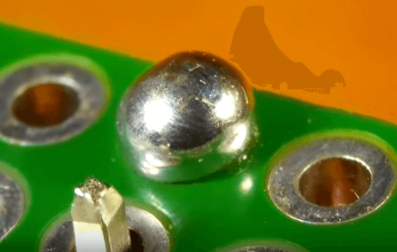
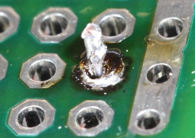
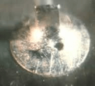
11. Solder Starved
(Source: Kitronik)
As its name suggests, a solder-starved joint does not have enough solder to form a solid electrical connection. The solder does not form a smooth transition surface. Here, it is likely that insufficient heat was applied to the lead, resulting in a poor connection. There are many reasons for Solder Starved, including:
- poor solder fluidity or premature solder withdrawal.
- Insufficient flux.
- The welding time is too short.
It is possible that this joint will work as there is still electrical contact made. But the mechanical strength is not high. Nevertheless, a solder-starved joint is likely to fail eventually as cracks develop over time and weaken the joint. Fortunately, rescuing a solder-starved joint is not difficult. Simply reheat the joint and add more solder.
12. Solder Splashes/Webbing
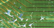
Soldering splashes on the traces (left) and around surface mount components (right)
(Source: Workmanship.nasa & Texas Instruments)
These bits of solder stick onto the solder mask in untidy splatters, giving the appearance of a spider’s web. These irregularly shaped threads are caused by insufficient use of a fluxing agent or the existence of pollutants on the surface of the boards during wave soldering. Unstable soldering iron temperature can also cause this phenomenon.
Solder Splashes/Webbing threaten to cause shorts.
If it is because there are too many rosin-type fluxes in the solder wire, it is recommended to reduce the amount of solder wire additives. If it is because the temperature of the soldering iron is unstable, it is recommended to use a constant temperature soldering iron table. Of course, keeping the surface of the boards clean is also important.
13. Pin Holes and Blow holes
A pin hole defect (left) and a blow hole defect (right)
(Source: eptac)
Pin holes and blow hole defects can be easily recognized as they appear as a hole in a solder joint. The terms pin or blow hole will give a clue to the size of the hole, with pin referring to small holes and blow holes being much larger holes. Rather than being a result of bad hand soldering skills, pin and blow holes are usually formed during the wave soldering process. Moisture within the boards is heated into gas during the soldering operation, and escape through the solder when it is still in a molten state. Voids are formed when the gas continues to escape when the solder joint solidifies. The circuit will conduct temporarily, but it is easy to cause poor conduction for a long time. Some ways that are employed to avoid this problem is by baking or preheating the boards to take the moisture out, and having a minimum copper plating thickness of about 25um in the through-holes.
What can you do to avoid soldering problems?
While there is no foolproof method to completely prevent soldering problems, there are some good habits we can adopt during PCB design and soldering to reduce the risk of running into soldering issues.
1. Consider solder mask design
Typically green in color, the solder mask the thin polymer coating applied to the surface of PCBs to protect the copper from the environment. Of course, the solder mask can also be displayed in different colors, including green, white, blue, black, red, yellow, etc. In particular, the solder mask not only plays the role of a solder mask but also plays the role of anti-corrosion, anti-moisture, and anti-mold. Besides preventing oxidation, they also function to prevent solder bridges from forming as well, as the solder does not adhere well to the coating. Hence, a solder mask can be designed between pads to form a solder mask dam. This is especially helpful for ICs and BGAs where the gap between pads can be as small as a few thousandths of an inch.
2. Place Fiducial marks
Fiducial marks are round solder mask openings with a round bare copper in its center, that are placed on your PCB board during the PCB design stage. There are panel fiducial marks and individual component fiducial marks for components requiring special treatment. Pick-and-Place machines see them as reference points on the PCB to align SMD components on your board during assembly. When used correctly, placement accuracy can be improved. Similarly, if fiducial marks are poorly designed (e.g. poor placement or not enough fiducials), they can lead to poor orientation, increasing the risk of soldering issues.
(Source: pcb-3d)
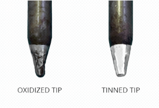
3. Cleaning and Tinning the tip of your solder iron
Poor tip maintenance is one of the leading causes of badly hand-soldered joints. Any contaminants or oxidation on the tip would decrease the solder iron’s ability to conduct heat, which in turn would reduce the quality of your solder joints. Hence, it is important to care of your solder tips. Before you start soldering, remember to clean the tip of your iron by rubbing it against a cleaning pad. If your soldering tip is already badly oxidized, you can use a tip activator to rescue it. Simply dip it into the paste-like substance, move it around and let the abrasives do their work, and the surface will be shiny again.
After that’s done, the tip of your iron should also be tinned. Tinning the tip of your iron means to coat the tip with a layer of solder to protect the tip from oxidation and to improve its ability to conduct heat. Clean and tin your solder iron tip after every two or three joints soldered, and another one time at the end of each soldering session. Doing so would extend the life of your soldering iron and improve the quality of your solder joints!
(source: weller-tools)
4. Practice makes Perfect
Soldering is a skill that gets better as you practice more! You can practice as much as you like on an old circuit board or a soldering practice board, before you embark on real projects that are too precious to ruin. Try out a variety of techniques, find a way for the solder iron to best fit in your hand, gauge how long you have to keep the solder and tip in place and make tons of mistakes.
To make solder practice more convenient, Seeed has rolled out a pen-like miniature soldering iron. With the temperature display and the control circuitry integrated into the grip, it makes soldering an even more fun and seamless experience.
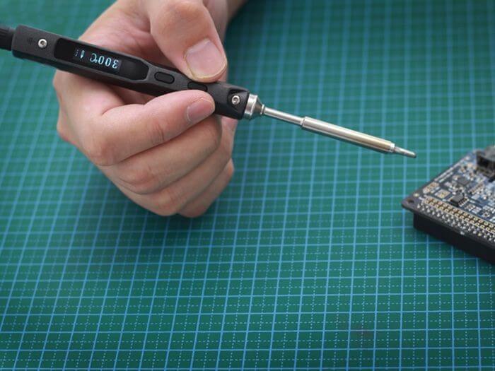
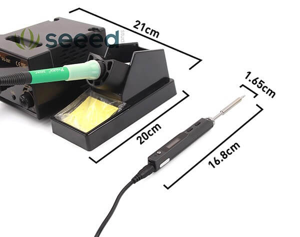
Ditch your heavy soldering irons for this miniature one!
5. Work with a Good PCB Assembly House
If hand soldering and sourcing for your own components is too much of a hassle, or if you think working with tiny components is beyond the abilities of your mere mortal eyes, there is always the option of working with a professional PCB assembly house who are experienced and familiar with the pitfalls of PCB assembly. Seeed provides a full turnkey service, including parts procurement and assembly. Whether you are prototyping or scaling up to mass production, Seeed Fusion is the one-stop destination for smooth and hassle free PCB Assembly.
We offer various sponsorships and value-added services to provide an unrivaled PCBA experience aimed at minimizing setbacks and maximizing yield and efficiency while supporting developers. We include PCB DFM and PCBA DFA design checks, and functional testing for one piece free with every PCBA order, and offer free prototyping for business users and additional sponsorships for Raspberry Pi CM4, Raspberry Pi Pico, and Wio RP2040 designs.
Get an instant online quotation now, we look forward to working with you.
“To make solder practice more convenient, Seeed has rolled out a pen-like miniature soldering iron. ”
Where can I find this iron?
Hi David, here you go: https://www.seeedstudio.com/Mini-Soldering-Iron-US-Standard-Shape-BC-p-2494.html