Dry Solder Joints in PCBA: Signs, Causes, Detection & Prevention
Solder can be present on a PCBA without forming a reliable connection. The resulting faults may be intermittent or appear after vibration or temperature changes, making troubleshooting and rework more difficult.
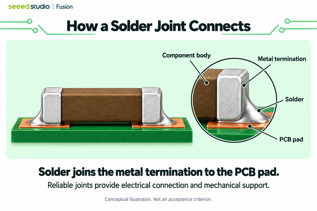
Understanding dry solder joints starts with how a solder joint connects a component to the PCB. This article explains the visible signs that need attention, common causes, inspection methods, and ways to reduce the risk during production.
🔗 What Is a Dry Solder Joint?
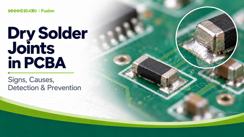
The term “dry solder joint” is commonly used to describe an unreliable soldered connection. Solder may appear to cover the joint, while the electrical connection or mechanical attachment between the component’s metal termination and the PCB pad remains poor.
For a chip resistor, solder connects the metal termination at each end of the component to its PCB pad. During soldering, molten solder must wet the metal surfaces and form a bond. Wetting describes how molten solder spreads over the surfaces being soldered. Surface condition, flux, and the temperature at the joint all affect this process.
The presence of solder does not confirm a reliable connection. Solder quantity, surface shine, and the overall shape of a joint cannot establish its quality on their own.
Inspection should distinguish between specific defects such as poor wetting, insufficient solder, and cracks. The term “dry solder joint” alone does not identify the exact defect or its cause.
🔍 How Can You Spot a Suspect Solder Joint?
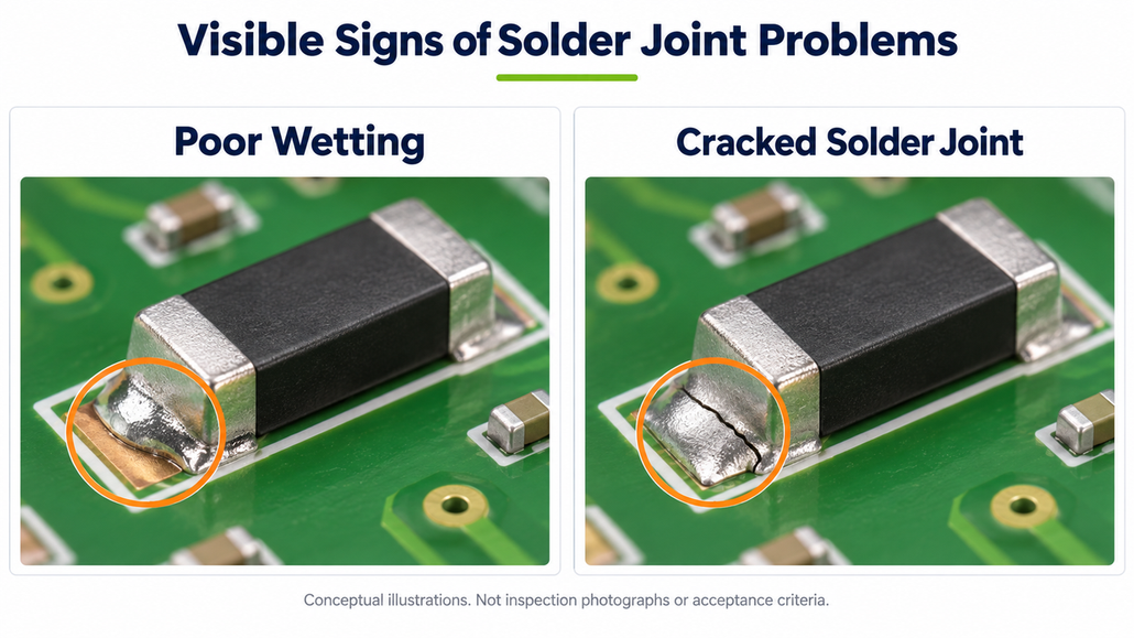
For visible joints, examine the areas where the solder meets the PCB pad and the component’s metal termination.
- Unusual edges or gaps: Solder may not spread continuously across the surface, leaving unwetted areas or visible separation at the connection.
- Cracks or damage: A crack in the solder or along the edge of the connection requires closer inspection.
- Unusual solder shape or coverage: Solder may form a pronounced mound or fail to cover the areas required for that component. Assessment should account for the package and the applicable acceptance criteria.
These signs help identify areas that need further inspection. Appearance alone cannot establish the cause. Poor wetting, insufficient solder, and cracks can all affect a connection, but each needs to be assessed separately.
A dull, rough, or less shiny surface alone is not enough to identify a dry solder joint. Solder alloy and process conditions also affect surface appearance. Inspect the connection areas and look for other signs of a problem.
Joint locations and shapes vary by package. Chip resistors, leaded components, and BGAs require different inspection approaches. A single solder joint shape cannot serve as a reference for every component.
⚠️ What Problems Can Dry Solder Joints Cause?
An unreliable soldered connection can cause an open circuit, abnormal contact resistance, or intermittent contact. At board level, this may result in startup failures, unstable signals, occasional interface failures, or functions that work inconsistently.
Some faults may not appear during the first power-on test. They can emerge after temperature changes, vibration, or a period of use. Intermittent faults are particularly difficult to troubleshoot because the same board may behave differently under different conditions.
Similar symptoms can also come from the power supply, components, connectors, or firmware. Inspection and testing are needed to locate the fault before attributing it to a solder joint.
📋 Common Causes and How to Prevent Them
Solder joint quality depends on the materials, metal surfaces, heating conditions, and what happens as the solder solidifies. Poor wetting is one common problem, and several factors can contribute to it.
| Possible cause | Effect on the joint | Prevention during production |
| Oxidation or contamination on PCB pads or component terminations | Oxides or contaminants interfere with contact between the solder and the metal surface, potentially causing poor wetting | Check solderability, follow storage and handling requirements, and limit contamination |
| Unsuitable flux or soldering materials in poor condition | Oxides may not be removed effectively, or the materials may not perform as required | Use materials compatible with the solder alloy, surface finish, and process; follow storage and use instructions |
| Insufficient heat at the joint or an unsuitable soldering profile | Solder may not fully melt, or the joint may not have enough time at the required temperature for wetting and bonding | Measure and verify the temperature profile on the actual assembly, then adjust the process as needed |
| Movement while the solder is solidifying | Movement of the component or board can disturb the connection, particularly during hand soldering or rework | Keep the connection stable until the solder has solidified and control movement and vibration |
🧪 How Can You Check Further?
The inspection method depends on whether the joint is visible, the component package, and the reported fault.
Visual inspection and AOI can check exposed solder joints and component placement. They help identify unusual connection edges, solder coverage, and other assembly problems. Suspect areas may require manual review or additional inspection.
For BGAs and similar packages, the joints sit underneath the component, where visual inspection and AOI cannot directly see them. X-ray can reveal features such as solder bridges, voids, and unusual solder distribution. However, an X-ray image cannot confirm every aspect of connection quality.
ICT checks electrical connections and component parameters within its test coverage, helping detect faults such as opens and shorts. Functional testing, or FCT, powers the board and checks the functions specified in the Test Plan.
Visual inspection, electrical testing, and functional testing provide different information. A passing result means the board met the criteria covered by that test under those test conditions. Intermittent faults may require further investigation under the conditions in which they occur.
For more about the scope of each method, see PCBA Quality Control: Flying Probe, AOI, X-Ray, ICT and FCT Explained.
🛠️ What Should You Do About a Suspect Joint?
Use the fault location, visual findings, and test results to identify the problem before deciding whether rework is appropriate. The aim is to determine where the connection has failed and which material or process conditions may have contributed.
The rework method depends on the defect and the condition of the component and board. It may involve cleaning, applying suitable flux, reheating the connection, or replacing a damaged component. Adding solder to the surface may leave oxidation, contamination, or a poor bond unresolved.
Control heating during rework to avoid damaging pads, components, or the PCB through repeated heat exposure. After rework, inspect the joint again and repeat the relevant electrical or functional tests.
If the same problem repeatedly occurs at the same location across a batch, investigate shared factors such as material condition, pad design, component solderability, the temperature profile, or handling. Reworking individual boards addresses the immediate faults; future production also needs changes that address the cause.
✅ Plan for Soldering Quality Before Production
Reliable solder joints depend on materials, design, process control, and inspection. Complete production files and clearly defined functional test requirements help the manufacturing team understand the assembly and plan suitable checks.
Seeed Fusion provides PCB fabrication, component sourcing, PCBA assembly, and inspection and testing services. The checks and tests used depend on the board design, component packages, and project requirements.
If your project requires functional testing, include a Test Plan with the test steps, required files, and pass/fail criteria. This allows production testing to check the functions your product needs.
Explore Seeed Fusion PCBA Testing Services, or submit your Gerber, BOM, and assembly files through the PCB/PCBA order page.
About Author
