Tombstoning in PCBA: Causes, Troubleshooting & Prevention
🔍What does tombstoning look like?
After reflow, a chip resistor or capacitor may have one end soldered to its pad and the other lifted off the board. This defect is called tombstoning. Even a slight lift can break the connection and leave an open circuit.
Check the part from the side if you can’t see both joints clearly from above. A shifted component may still sit flat, and a flat component can also have a poorly wetted joint. For more on solder joint defects, see Dry Solder Joints in PCBA.
🌡️Why does one end lift during reflow?
As the solder melts, it spreads over the pads and the metal ends of the component. This is called wetting. The surface tension of the molten solder pulls on the component at both ends.
When both ends wet at about the same time, the forces tend to balance. If one end wets first, the pull on that side can tip the part and lift the opposite end off its pad. Small parts such as 0402 and 0201 resistors and capacitors are particularly sensitive to differences in paste deposits and placement.
📋What to check and how to prevent it
Start by comparing the two ends of the affected part. Follow the same location from the PCB layout through printing, placement, and reflow.
| What to check | What to look for |
| Pads and copper connections | Compare the footprint with the component manufacturer’s recommended land pattern. If one pad connects directly to a large copper pour and the other to a narrow trace, the solder on the copper-heavy side may melt later. A thermal relief uses narrow copper spokes to limit heat flow into the pour. Check current and heat dissipation requirements before changing the connection. Also look for an open via within either pad, where molten solder can wick into the hole. |
| Stencil and paste printing | Compare stencil opening size, stencil thickness, and the actual paste deposits on the two pads. If the line uses solder paste inspection (SPI), check the volume and position of each deposit. |
| Component placement | Check whether the part is centered and whether both ends make contact with the printed paste before reflow. |
| Reflow profile | Measure temperatures on an actual board. Check whether the two ends heat unevenly and whether the profile meets the paste supplier’s recommendations and the components’ temperature limits. |
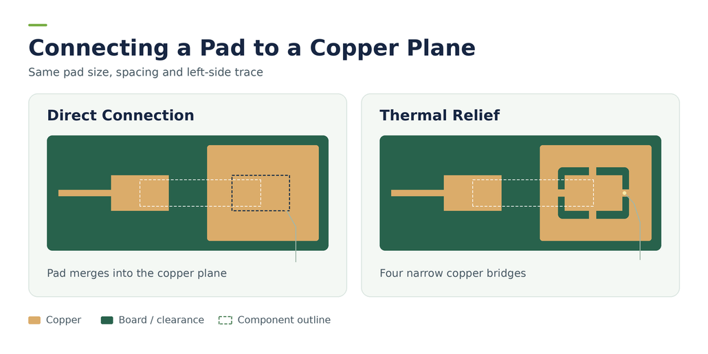
If the same location is affected on several boards, record the component reference, such as R12 or C5, and take photos from above and from the side. Compare the layout and production records for that location. After rework, inspect both joints and repeat any relevant electrical checks. For more on inspection methods, see PCBA Quality Control: Flying Probe, AOI, X-Ray, ICT and FCT Explained.
🚀Planning Your Next PCBA Build
Before assembly, Seeed Fusion’s Design for Assembly (DFA) review checks that the production files agree and that the specified components match their PCB footprints. After reflow, automated optical inspection (AOI) and manual review can spot visible defects such as a lifted component. If we find tombstoning during production, we assess whether the affected boards can be reworked. If the layout appears to be the cause, we’ll flag the affected location so you can review it before the next run. For details on the pre-assembly checks, see our PCBA DFA Review Guide.
For a pilot run or your next production batch, submit your Gerber files, bill of materials (BOM), and assembly files. If an earlier build had tombstoning, you can also share the affected component’s reference or a photo to help our engineers review that area.
Submit Your PCBA Files to Seeed Fusion →
About Author
